Advanced technologies of printed circuit boards
25.11.2015
The complexity of electronic circuits has been growing, and the emerging new technologies raise the bar for these products. The parameters of PCBs (printed circuit boards), which are components of electronic equipment, must also follow the demands. Hence PCB designers should be aware what solutions they can use, what are the advantages and limitations thereof, and how to make the best use of them.
This paper presents the advanced technologies and requirements applied in e.g. HDI circuits, as well as the applications of additional external coatings with non-standard machining methods. The finish of the article explains what parameters define the quality of manufactured PCBs.
Preservation and protection

Fig. 1. Example application of a peelable mask.
PCBs often work in harsh environmental conditions which require application of additional coatings (i.e. masks) to protect the products from ambient factors and improve their reliability. It is sometimes enough to provide temporary protection of selected PCB areas, e.g. for the assembly stage only, and this is applied especially when a PCB passes several cycles of automatic soldering. The areas are protected with peelable masks, an example application of which is shown in Fig. 1. It is a special coating the main function of which is protection of selected areas on a PCB (and inside its holes) from direct action of soldering and chemical processes, e.g. during automatic PCB assembly. They can be easily removed after processing and leave no residues.
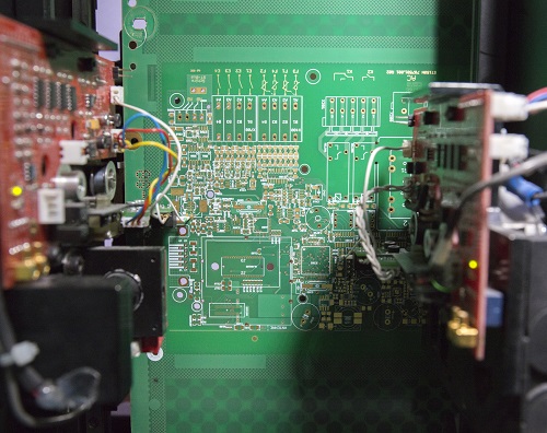
The PCBs that are assembled with manual control, keypads, LCD displays, etc. have the pad durability and conductivity improved with carbon prints (see Fig. 2). This coating is made of electrically conductive graphite paste that is silkscreened and cured. Some designers use the solutions as an additional and simple conductor layer located along the PCB outer.
Vias in some PCBs must be permanently protected against ambient conditions. This is done, for example, for protection against soldering, shorting, etc. when components are assembled directly over the vias and causes the risk of ingress of contaminants or solder. This issue is very critical in μBGA circuits. Designer may currently use many methods to obscure or fill the vias. The right method depends on the types of risks that must be prevented. The simplest solution is covered vias, where a soldering mask obscures them. This, however, does not guarantee proper filling. It only covers the ring and the inner walls. This provides a basic protection level that is mainly effective during soldering, since the solder cannot wet the via. More advanced methods consist in building plugged vias with special filling compounds that are cured in the manufacturing process, followed with a cover being a mask layer. This procedure protects the vias against all the hazards specified above.

Fig. 2. Example application of a carbon print.
Microvias and the press-fit process
The growing complexity of PCBs forces the use of techniques that guarantee intensified usage of PCB areas, e.g. microvias, which are holes 0.15 mm or smaller in diameter. Blind vias and buried vias are also used as microvias, and these are detailed in "Elektronik" issue 6/2013. The key advantage of those vias is that the interconnection density can be increased without adding more layers or making the PCB dimensions larger. This packing density is sometimes necessary also due to the required EMC of the designed device.
Electronic devices often come with connectors that provide electrical bonding of other device modules and allow fast module swapping, e.g. due to servicing reasons. Connectors cannot be soldered if their temperature resistance is poor. They are assembled with the press-fit process. This process comprises installation of the connectors by pressing them into dedicated vias that are made with reduced diameter tolerances (which is ±0.05 mm in standard). The press-fit process requires no specific design approach; still, design engineers should make sure that the PCB manufacturer knows exactly which holes must be dedicated for press-fit assembly.
Machining

Fig. 3. Example of z-routing.
One of non-standard machining of the FR4 laminates is z-routing, which is milling a specific laminate area down to a defined depth. Z-routing (see Fig. 3) permits assembly of atypical, tall components, countersinking of fastening bolts, or fitting a PCB in a non-standard (low) enclosure. When ordering PCBs that require z-routing, the PCB manufacturer must be provided with clearly specified sides and depths of laminate processing. Note that z-routing has its own processing tolerance, which is usually similar to that of regular milling. Techno-Service uses a tolerance of ±50 μm by default.
Another non-standard machining method is to metallize (plate) the PCB edges (see Fig. 4). Similar to vias, the edges can be plated to create a permanent and reliable conductive layer. This solution is mainly applied to improve EMC of electronic equipment. The process is also used to build adapters between the main PCB and a non-standard component (e.g. a later revision) or another PCB the assembly of which is not possible with standard processing. In this case the plated edges are made as half-holes left for downstream assembly. Yet another application of this process is its capacity to make custom edge connections.

Fig. 4. Example of a PCB with plated edges.
Relying on quality gives reliable PCBs
Many electronic devices must deliver high reliability. These demands are translated into the high quality of applied components, assembly and PCBs. The quality in this case is defined in various industry standards, the most relevant of which is the IPC standard series (A-600, 6010, 6012, 6013, etc.). The documents provide standardised and generally recognised acceptance criteria for PCBs. The standards divide the PCBs into classes of performance (build) quality that consider many parameters: minimum hole plating thickness, minimum conductor width, dimensional tolerances, etc. The majority of PCB manufacturers make PCBs in IPC Class II by standard. There are few PCB manufacturers, and this includes Techno-Service, offer PCBs of higher performance quality: Class III. If a designer wants a PCB of this class, they need to specify that in the purchase order.
The quality of PCBs may also be proved with the UL certificates that declare the non-flammability levels for the finished PCB and its materials. The highest non-flammability class is 94V-0, which means that the test sample removed from fire will self-extinguish in 10 seconds and the dripping molten material does not burn.
Due to the sheer extend of the subject, this article presents only the most common non-standard technologies found on the market and the basic introduction to the quality of PCBs. While the use of non-standard technologies may inflate the PCB costs, it often avoids assembly difficulties and operating problems with the finished device. If you want high quality PCBs, it is best to choose a manufacturer that has the technologies and quality parameters discussed herein. Cooperation with that PCB manufacturer, especially when supported by their great experience, will certainly prevent many design errors, which will save time and money. Moreover, the designer should be also well aware of the processing capacities of the vendor of choice and follow all changes in their range, while requesting for more processing solutions whenever needed.