
Buried and blind vias and using their advantages in electronic device projects
Łukasz Romik Author
The PCBs applied in modern electronic equipment grow in complexity: designers must pack more and more components on increasingly smaller surfaces. Buried and blind vias are enable miniaturisation with a simultaneous growth of complexity. These solutions have been offered by Techno-Service for years. In order to fully utilize the potential of vias, it is good to better understand their differences, principles of proper PCB design with the vias, and the benefits of the solution.
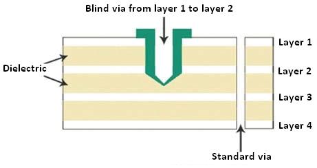
Fig. 1. Diagram of a PCB with blind via from layer 1 to layer 2.
The nomenclature of new technological solutions is immense. One of the main concepts is blind via. It is an opening that begins on the PCB surface and does not go all the way through to the other side. Blind vias can be machined by drilling or laser-cut. A blind via may connect the PCB top or bottom with an inner coating without piercing through the board.
The practical manufacturing has seen a growing use of buried vias in PCB design. Blind via PCBs are used when the designed PCB is extremely packed and the designer needs more space on the top or the bottom, or lacks room on one of the PCB sides and does not need to design a connection by a through hole.
Production of PCBs with blind or buried vias varies greatly from the standard PCB production processes. Blind via PCBs are made just like regular multilayer PCBs, up to the drilling stage. They feature additional holes that connect only two layers in a four-layer board.
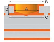
Fig. 2. Blind via hole (min. drilled hole size A = 0.15 mm, min. outer layer pad dia. B = 0.25 mm,
min. inner layer pad dia. C = 0.25 mm, D:A = 1:1).
The holes are not bored through, hence the blind vias. Drilling the holes down to the copper layers inside the PCB allows building an electrical connection between two layers only once the hole has been plated. This largely improves the PCB capacities and application range.
The solution provides multiple benefits: a higher density of SMT components (the vias do not take up all layers) and better product safety from the improved quality of electrical insulation. Sooner or later every multilayer board designer faces the need to use non-through holes. Unfortunately, no uniform standards have been developed so far for the design and production of blind vias.
The capacity to produce the vias depend on the processing solutions applied by specific multilayer PCB manufacturers. Nevertheless, several general principles can be defined that allow designing PCBs in a way that will permit its production in nearly all modern multilayer PCB manufacturing facility.
How to design
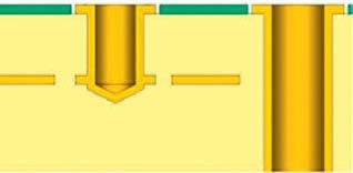
Fig. 3. Plated blind via.
When a designer starts developing a multilayer PCB the first step will be to choose the build-up. The decision of what build-up to use should be made already in the beginning of the design process, and the design assumptions should be consulted with the PCB manufacturer beforehand.
Designers who plan holes in multilayer PCBs often only consider their idea of the design without regard for the processing capacities of the manufacturer, or add vias ‘on the go’, when they run out of the board space, and adapt them to the demands of the design nearly right before its pressing.
The consequences of such approach may be dire for the designer, who can be ultimately forced to redesign the entire circuit, or for the entire business – loss of money and time will be unavoidable to find the PCB manufacturer, with increased order costs and lead times. Some unreasonable designs cannot be built at all by any existing PCB production plant. Sometimes the PCB production costs overrun the project budget.
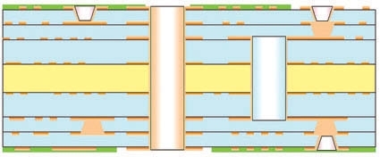
Fig. 4. Buried via and blind via.
To conclude, when planning the build-up, the designer’s key duty is to optimally combine the requirements of the target device with the processing capacities of its manufacturer. The selection of materials and layer thickness is a different subject altogether. The PCB manufacturers try to define PCB design rules that will make the PCB manufacturable. Hence it is important to study the design principles for blind and buried vias.
Blind vias in multilayer PCBs connect the outer data layers with one or more inner layers. Drilling blind vias to a designed depth is complicated by certain processing limitations. Proper metallization (plating) quality requires proper selection of the via sizes: the H/d value (bore depth to bore diameter) must not exceed 1, and 0.8 is optimal. This means that the deeper the via gets (and thus the dielectric gap between the layers), the larger its diameter should be.
The multilayer circuit design process must consider the fact that buried via plating results in copper deposition (at +24 to +45 additional micrometres) on the specific layer surface. Extra plating deposition on those layers must be then considered when planning the minimum permissible path thickness.
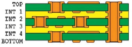
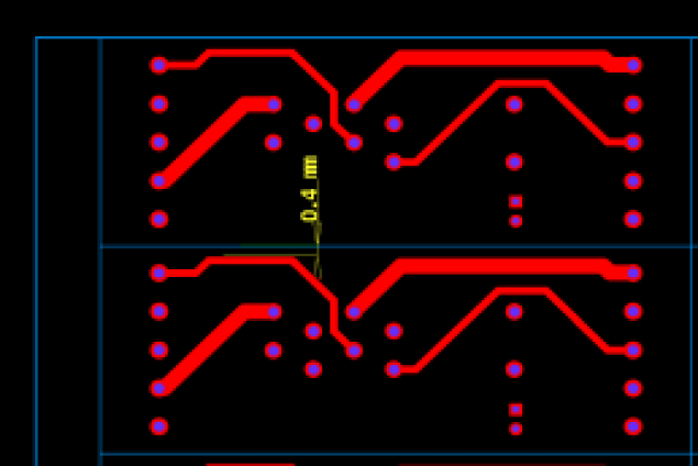
Fig. 5. Buried and blind vias in a 6-layer PCB.
The manufacturing process for the vias is not unlike in typical PTH’s followed by compound filling and pressing into a complete multilayer circuit pack. It is not possible to build microvias directly over buried vias, since there is no firm surface at those locations – instead, there is a metal ring with a hole in the middle.
The production of the structure is: first, holes are drilled through and each core is plated. Next, the mosaic image is deposited on the inner surface of the cores, and the multilayer pack is pressed. Production-wise, the structure of the process is not optimum because additional metal plating stages are needed. If the PCB facility has no machinery for microvia drilling, this is the only way to build those holes.
Variations in the number of layers of multilayer PCBs with buried vias can be different, but the complexity of the PCB or the number of buried and blind vias should never be too high. If a choice between making yet another blind hole and an additional pair of layers can be made, the latter option is better. Specifically, BGA IC’s with the raster at 1.0 mm or even 0.8 mm do not require blind holes. BGA IC’s with the raster at 0.65 mm and 0.5 mm must feature blind holes. Unfortunately, no alternative solution exists. In any case, the build-up of multilayer circuits should be consulted with the PCB manufacturer beforehand.
Summary
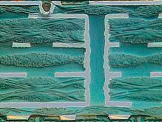
Fig. 6. Cross-section of a PCB with a buried via.
The application of microvias and blind vias that connect several circuit layers, as well as buried vias may increase the interconnection density by several times without increasing the number of layers. The PCBs built that way are often cheaper from their counterparts due to the interconnection density on standard PCBs with pass-through holes. An example 4-layer board with blind microvias allows an interconnection density equal to that in a 10-layer PCB with pass-through holes. The price of the 10-layer PCB will be 100% to 150% more expensive than the HDI 4-layer PCB.
The expensive and difficult task of manufacturing PCBs with blind and/or buried vias is an opportunity for development of electronic devices and assures more stable operating conditions of the circuits with improved performance. Although the new technologies were feared and extremely expensive in the past, the latest research and advancements in the field have eliminated nearly all drawbacks. In reality, blind and buried vias seem to dominate in high-technology PCBs due to the high density of packing per board, which is a very cost-effective alternative to traditional through vias.
Show more from category PCB documentation
-
PCB documentation

Integr8tor - problems solving
-
PCB documentation

Integr8tor—project processing
-
PCB documentation

Automated Analysis of PCB Designs - the process of creating production documentation
-
PCB documentation
How to optimize machining of printed circuits? - part 1
-
PCB documentation

Bridges – structure and parameters
-
PCB documentation

What to remember while designing multilayer PCBs?
-
PCB documentation
Accepted file format for printed circuit board designs
-
PCB documentation
How to correctly design panels for small circuits? - part 2
-
PCB documentation
How to correctly design panels for small circuits? - part 1
-
PCB documentation
Proper preparation of copper layer
-
PCB documentation

Proper preparation of solder mask layer
-
PCB documentation

Proper preparation of PCB outline