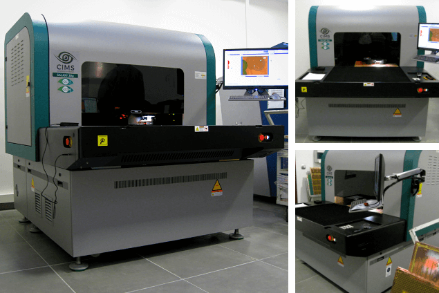
The machinery stock: CIMS Galaxy AOI Systems optical tester
2020-02-12The CIMS Galaxy AOI Systems optical tester is the first TS PCB investment in the machinery stock this year. The purchase of the new machine starts the implementation of this year's plans related to the development of the machinery stock and the increase in the production capacity of the plant.
In 2019 we opened a new part of the production plant, and now it is time to invest in the technological development of TS PCB - emphasises TS PCB Director, Mr Andrzej Wałachowski. The first phase of this project is the purchase of the CIMS Galaxy AOI Systems tester, whose full integration into the production process was finalised in January 2020. The value of the whole project amounts to nearly 15 million PLN, and all purchases and accompanying implementation works have been planned for the next two years. During this time, we intend to implement, among others, new technologies for mask application and exposure and to implement another galvanic line in the process.
As a result, we will be able to offer our customers the production of more technologically advanced circuits, and our production process will be even more efficient than before. Thus, we will combine advanced technological solutions with the agile manufacturing concept. We hope that in this way we will not only strengthen our leading position in the Polish market but also gain new customers outside our country.
The main technical features of the device are as follows:
- the analysis and measurement of paths with an accuracy of +/-10 μm on the surface of the entire form and the detection of copper losses in paths or short circuits between them;
- the analysis of the mosaic image of the actual circuit, which will be compared with the reference one generated from the circuit design documentation;
- the possibility of detecting critical mosaic damages and defects in their execution at several stages of the technological process: e.g. drilling and milling before etching, photochemistry, galvanic copper plating, the etching of mosaics;
- the possibility of detecting, among others, the shifting of the drill hole, the occurrence of necking and thickening of paths, too thick metallization, overbiting and underbiting, surface scratches;
- locating mosaic anomalies and potential anomalies at certain stages of circuit manufacture that cannot be detected by electrical testing.
The implementation of the new machine will make the testing process even more reliable. Our customers will be guaranteed a supply of fully functional circuits in which all potential irregularities will be excluded.