


08.10.2018
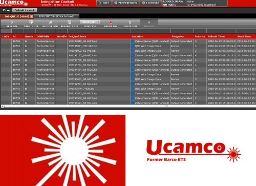
Integr8tor - problems solving
If operator intervention is required during the analysis of technical documentation, processing in Integr8tor (I8) is stopped and the project is marked as being resolved. After selecting the project, a list of encountered problems is visible (Fig. 1). Some of them are the result of incorrect recogni...
11.09.2018
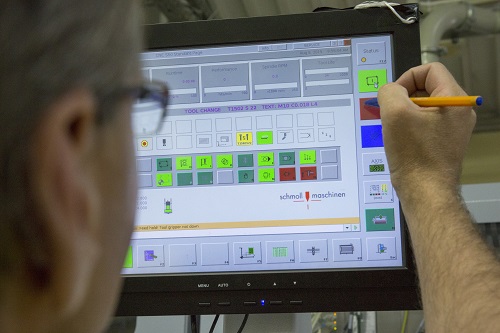
Integr8tor—project processing
The current capabilities of artificial intelligence, and above all machine learning techniques, combined with the high computing power of modern computers, allow you to analyse, search and classify information in large data streams.
The use of this potential for automated analysis of CAM documen...
14.08.2018
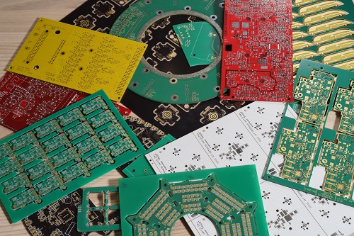
Automated Analysis of PCB Designs - the process of creating production documentation
The time of order fulfilment and the speed of delivery of price offers constitute in the PCB industry one of the main factors that determine the choice of manufacturer. Shortening the physical processes occurring during the production of circuits is very difficult, sometimes even impossible. It is r...

28.09.2017
How to optimize machining of printed circuits? - part 1
The final stage of the printed circuits production is machining.
They reach its final shape during milling and scoring process. Improperly designed machining can distinctly increase the production costs and extend the awaiting time for delivery of the final product, especially in case of orders...
28.06.2017
Bridges – structure and parameters
If PCBs are made in panels and scoring cannot be performed, PCBs are held using so called bridges.
If the order does not specify their parameters, perforated bridges are normally installed. Keep in mind that the minimum distance of traces, pads, or compound from the perforation hole e...
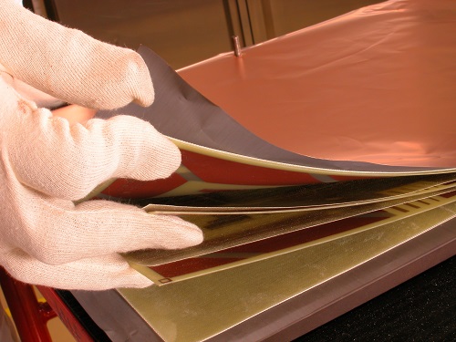
06.06.2017
What to remember while designing multilayer PCBs?
The structure of multilayer PCBs is much more complex than PCBs with one or two copper layers.
Some aspects of their construction should be considered at the designing stage.
Below some general advice is provided to avoid the most common problems, which arise both at production and...
25.05.2017
Accepted file format for printed circuit board designs
The commonly accepted file format for printed circuit board designs is the Extended Gerber RS-274X with drilling files in Excellon format.
Most of PCB manufacturers also accept the following file formats:
Gerber RS-274X2
ODB++
Eagle BRD (up to 4 layers)
Mania-Barco...
.png)
17.05.2017
How to correctly design panels for small circuits? - part 2
Routed and v-cut scored panels
Each circuit form, unless rectangular, necessitates routing. V-cut scoring is necessary if circuits in the panel have at least one vertical or horizontal edge; in such a case it will be possible to route the remaining edges.
Mixed processing (Photo...
.JPG)
09.05.2017
PCB design – only Eagle?
One of the most popular tools for designing printed circuit boards includes EAGLE software. The Autodesk company that has been administrating it since last summer have decided to introduce a subscription for users. Until now, a one-off licence purchase (USD 70 for the standard version, USD 800 for...
.png)
27.04.2017
How to correctly design panels for small circuits? - part 1
Directions of development in the manufacture of electronics exhibit a progressive trend towards the miniaturisation of electronic equipment with a simultaneous increase in its functionality. The tendency to miniaturise devices is already widely known and this is related to the reduction of physica...
30.11.2016
Proper preparation of mosaic layer
A sporadic mistake in printed circuit boards is when the design exceeds the minimum DRC (Design Rule Check) parameters. These parameters define the technological possibilities of a printed circuit board manufacturer with regard to the minimum track width, the distance between adjacent tracks / pad...
30.11.2016
Proper preparation of solder mask layer
A common mistake in printed circuit board documentation is an incorrectly prepared solder mask layer.
Its correct implementation make it possible to eliminate problems at the PCB production stage and also in the process of component installation in circuits. It is inappropriate to pre...
.png)
23.06.2016
Proper preparation of PCB outline
A common mistake in printed circuit board documentation is an incorrectly prepared outline layer.
A properly prepared outline is shown in Fig. 1 – the line with constant width clearly indicating the printed circuit perimeter edge. Fig. 2 additionally shows it paired with a mos...
08.02.2016
PCBs production documentation – how is it created and what are its contents?
While designing a printed circuit board, the designer develops a vision of a printed circuit of which the connection network will ensure its correct and faultless operation. This vision is reflected in the electronic version of the design, prepared in a CAD program, and the design documentation ge...
25.11.2015
Thick copper layers in printed circuit boards. Application and design
Printed circuit boards (PCBs) are most often used in low-voltage electronic systems and devices, which are products that have been continuously minimised in size by reducing the dimensions of mosaic components. PCBs have been increasingly used in high current power devices with electrically conduc...

25.11.2015
Printed circuits. Typical errors in production documentation. Part 2
The first part of the article (see "Elektronik" issue 3/15) is dedicated to the characteristics of good production documentation and the popular file formats used in the PCB industry. Typical errors of project/design documentation were also discussed as exhibited on mosaic, resists and t...

25.11.2015
Printed circuits. Typical errors in production documentation. Part 1
The contents and quality of electronic production documentation for printed circuit boards (PCBs) is decisive to the time and cost of finished PCB production. Vague and imprecise information often leads to great problems in proper interpretation of actual customer requirements and, in extreme case...
25.11.2015
Methods of printed circuit board pricing optimisation
The design of printed circuit boards (PCBs) can be defined as a process of seeking the best layout of the connection networks for circuit components and electronic devices while retaining the desired levels of electrical parameters, e.g. impedance of differential transmission lines, thermal parame...
25.11.2015
How to prepare a good production documentation, or what design engineers must know when working with PCB manufacturers
The cooperation between the PCB designer and the PCB manufacturer is extremely critical. The better the first order delivery stage is prepared, the shorter is the time to receive PCBs that meet customer's specification. A production documentation that is vague or unclear will extend the time t...
25.11.2015
Buried and blind vias and using their advantages in electronic device projects
The PCBs applied in modern electronic equipment grow in complexity: designers must pack more and more components on increasingly smaller surfaces. Buried and blind vias are enable miniaturisation with a simultaneous growth of complexity. These solutions have been offered by Techno-Service for year...

