


22.11.2018
TS PCB – towards the Industry 4.0
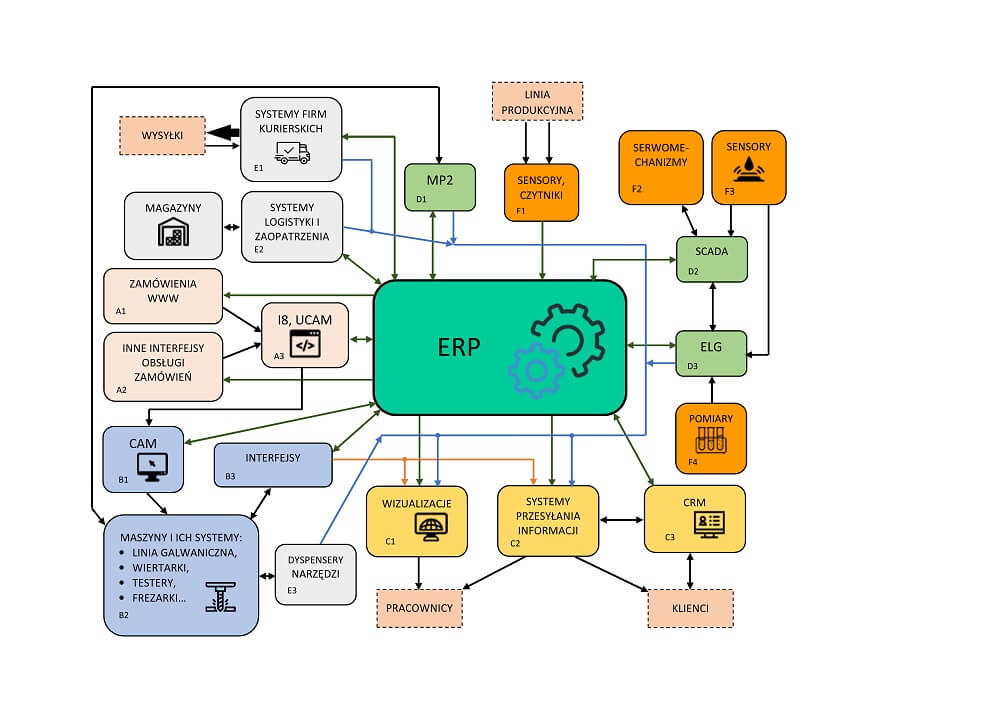
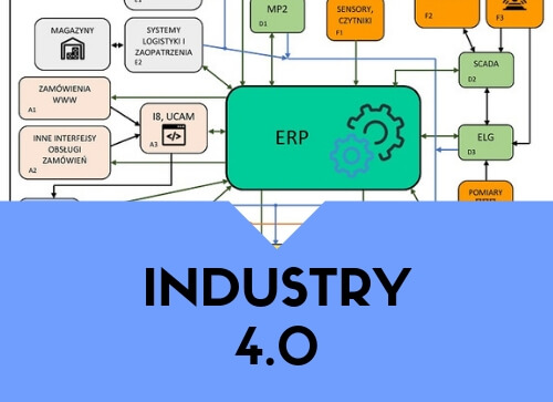
The enormous development of broadband Internet technology, of wireless communication, together with the increase in the computing power of computers and microsystems, which has been observed for over ten years, has created new opportunities in many areas of life. One of the results are the smart dev...
22.11.2018
Industry 4.0
"Smart factory" is a slogan that has been appearing for a long time in foreign trade press. It is also being more and more often mentioned in the context of polish industry. Full automation of production seems to be the only right direction for the development, the fact that is slowly beco...
16.05.2018
Standard structure, non-standard application of PCBs
With the use of typical elements, such as tracks and metallised holes, one can realize more complex technological solutions on the surface of a printed circuit.
The first atypical application of the printed circuit, which is worth mentioning, is the creation of integrated modules that a...
18.04.2018
Unusual applications of printed circuit boards and laminates
A printed circuit board is most likely defined as copper track layout placed on both sides of the dielectric substrate, connected by appropriately located metallic through holes (Fig.1).
Fig. 1
Its essential features are especially durable and accurate representation of...
04.01.2018
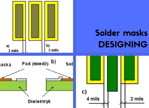
Solder masks in printed circuits - designing
Masks are prepared as negative layers so any components placed on them will in fact be areas free of paint. Typically these are SMD pads or assembling holes which can be defined in two ways (fig. 1):
- by copper which means that the mask does not influence the pad size — the opening is larg...

27.12.2017
Solder masks in printed circuits - performance specifications
The specification most often charactering the mask’s performance is it thickness.
In the case of a wet mask, it is a maximum of 40 µm ÷ 50 µm (thickness in mass areas) assuming that it is applied to copper with a typical thickness of 35 µm. The mask has a...
27.12.2017
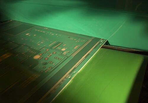
Solder masks in printed circuits - application process
The solder mask (wet) is applied to the surface of the circuits using two methods: screen printing and photo printing.
Screen printing consists in applying the mask image by means of a screen and then hardening it thermally or with use of UV radiation.
In the photo printi...
18.12.2017
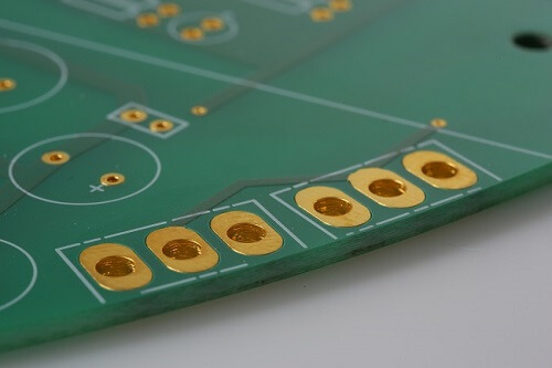
Solder masks in printed circuits - types and basic functions
Mosaics of printed circuits are made from copper whose major advantage is excellent conductivity of electrical current and heat. At the same time, this metal is susceptible to the adverse effects of oxidation when in contact with air and moisture. In order to protect mosaics from environmental impac...
28.09.2017
Milling of circuits edges – definition, methods of chamfering
Milling is a sloping edge cutting of laminate (execution of the so-called phases), mostly edge joints. In TS PCB, there are two ways to execute this type of machining:
Milling with the depth milling method.
With this method, one can mill almost any edge of PCB. The main limitation is the...
10.08.2017
Vias types according to IPC standard
Beside the PCB manufacturers recommendations and guidelines coming directly from customers the requirements concerning embodiment of the printed circuits are also contained in a series of IPC standards, in the IPC 4761 standard among others – which shortly concerns the vias protection.
&nbs...
04.08.2017
PCB elements: HOLES TYPES
Due a big variety of functions and applications of printed circuits the different types of the holes can be present in their structure. They can be classified in a general way – metalized / non-metalized or because of their shape or function etc.
The classification considering most ty...
28.07.2017
Parameters of printed circuits _ ELECTRICAL
Apart from the basic and temperature parameters listed above, laminates may also be described with electrical parameters (apart from CTI mentioned above), water absorption resistance and CAF.
Electrical characteristics:
From the electrical point of view laminate...
19.07.2017
Parameters of printed circuits _ TEMPERATURE
For protection against the adverse influence of elevated temperatures laminates with appropriate temperature properties should be used for producing printed boards as they adapt both to the assembly process and to the conditions in which a ready-made device operates.
Definitions of th...
07.07.2017
Parameters of printed circuits _ BASIC
The most basic parameter of a printed circuit is the type of laminate i.e. the base material for production.
Out of all the materials available on the market, it is FR4 i.e. epoxy-glass laminate that enjoys the greatest popularity. It meets the vast majority of needs on the...
22.06.2017
Manufacturing printed circuit boards – now and then, part 2
Looking through the TS PCB TECHNO-SERVICE S.A. archives, we found a photo of a brushing machine we used in the 80.
Photo: brushing machine_archive TS PCB TECHNO-SERVICE S.A.
The machine we are currently using enables us to reduce the number...
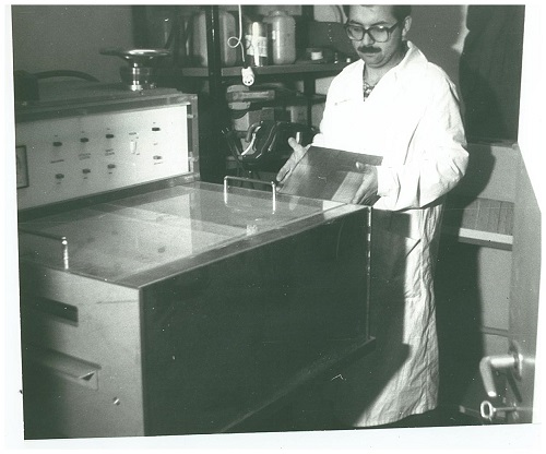
22.06.2017
Manufacturing printed circuit boards – now and then, part 1
Does anyone still remember AWS-1 NC driller?
When TS PCB TECHNO-SERVICE S.A. was initiating its production activity in 1985, it was a jewel among our machinery.
Photo: awS-1 NC drill_archives TS PCB Techno-Service S.A.
Now nothing reminds us...
06.04.2017
Construction of multi-layer PCB's
Core, prepreg & copper foil.
Multi-layer printed circuits, when compared to single or double-layer circuits, exhibit a more complex layer structure.
An example stackup is shown in Fig. 1 which presents the layer stack of a typical 4-layer circuit. It is made up of three basic...

