
Automated Analysis of PCB Designs – the process of creating production documentation
Łukasz Romik Author
The time of order fulfilment and the speed of delivery of price offers constitute in the PCB industry one of the main factors that determine the choice of manufacturer. Shortening the physical processes occurring during the production of circuits is very difficult, sometimes even impossible. It is relatively easier to optimize the time of pre-production stages. The longest of them is the one related to the preparation of production documentation.
The current article presents a technique for accelerating pre-production processes through the use of the Integr8tor software, which was implemented at TS PCB in early 2018.
Preparation of production documentation takes place in two stages:
1. Initial verification of the project’s design documentation.
It involves, among other things, verifying the completeness and readability of project files, as well as checking the matching of layer images.
2. Verification whether the project parameters correspond to the technology declared in the technology card.
One compares, among others, the number of copper layers, of anti-soldering masks or descriptions. The resulting non-conformities are explained to clients until the documentation raises no objections as to its completeness and correct interpretation.
The most labour-consuming element of the initial verification is loading of documentation generated by various CAD programs and interpreting the purpose of its various layers based on many naming schemes. The wide variety of file formats and naming of individual layers can lead to mistakes and extend the analysis time.
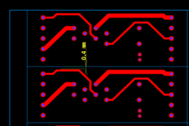
The initially verified project goes then to the CAM department, where the proper production documentation is developed. In outline, this process involves the verification and possible matching of projects to the technological requirements of the production line and the creation of electronic documentation, in the form of, among others, software for plotting film or a device for direct exposure Ledia ( DLI – Direct Laser Imaging), machining and optical and electrical testing. The most time-consuming activities are loading in the documentation and setting the layers, as well as checking the DRC parameters of the DRC mosaic ( Design Rule Check). DRC control is extended for complex multilayer circuits, especially of the HDI type (High Density Interconnect). It mainly includes determination of the three characteristic parameters for mosaics of external and internal layers (Fig.1):
- the minimum distance (gaps) – the smallest Euclidean distance between the mosaic elements within own or neighbouring network,
- minimal track width—the smallest width of mosaic elements forming electrical networks,
- minimal annular ring—the copper area around the metallised hole. Usually, the width of the ring is half the difference between the diameter of the pad and the metallised hole placed in it.
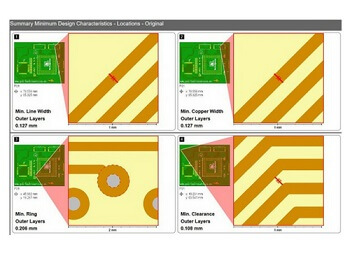
Fig. 1. View of the mosaic parameters window.
Time-consuming for determination of DRC parameters is also increasing for projects in which contact pads are not created using dedicated apertures, but are outlined by paths. Another factor that lengthens the time required for defining the DRC is painting large areas of masses with 1-2 mils thicknesses, instead of contouring them.
Show more from category PCB documentation
-
PCB documentation

Integr8tor - problems solving
-
PCB documentation

Integr8tor—project processing
-
PCB documentation
How to optimize machining of printed circuits? - part 1
-
PCB documentation
Bridges – structure and parameters
-
PCB documentation

What to remember while designing multilayer PCBs?
-
PCB documentation
Accepted file format for printed circuit board designs
-
PCB documentation
How to correctly design panels for small circuits? - part 2
-
PCB documentation
How to correctly design panels for small circuits? - part 1
-
PCB documentation
Proper preparation of copper layer
-
PCB documentation
Proper preparation of solder mask layer
-
PCB documentation

Proper preparation of PCB outline
-
PCB documentation
PCBs production documentation – how is it created and what are its contents?