
How to correctly design panels for small circuits? – part 1
Łukasz Romik Author
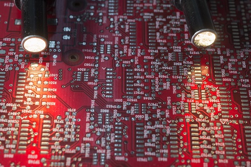
Directions of development in the manufacture of electronics exhibit a progressive trend towards the miniaturisation of electronic equipment with a simultaneous increase in its functionality. The tendency to miniaturise devices is already widely known and this is related to the reduction of physical sizes of printed circuit boards which directly influences the production and assembly process.
Circuits of size 50 mm and smaller should be produced in panels. When designing them two decisions need to be taken: the optimal layout and number of circuits, and the selection of appropriate mechanical processing method taking into account size, form of single boards and laminate thickness. Designers very often fail to see very important issues i.e. keeping the correct layout of copper in circuits and the panel frame. A correctly designed panel guarantees the optimal assembly of elements and the easy separation of the assembled circuits with the least complex production process. It also guarantees the integrity of circuits in the production process and when transporting panels to an assembly specialist.
Rules for correct panel laying for small circuits, based on the experience of engineers from the CAM Company TS PCB Techno-Service will be described further in this article. Knowledge of these issues can bring about advantages in:
– improving the mechanical stability of the panel,
– optimisation of the assembly process,
– separation of circuits
– reduction in board production costs.
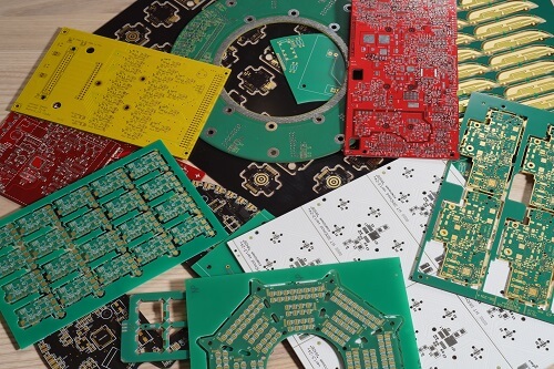
Small circuits
Mechanical processing constitutes one of the significant limitations in producing small and individual printed circuit boards. It allows one to freely separate the boards from the production format.
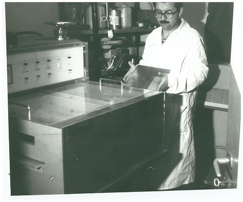
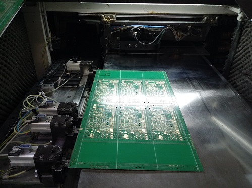
The minimum size of individual circuit boards in TS PCB Techno-Service S.A. should be 30 x 30 mm. This size results from the characteristics of mechanical processing. During routing (Photo 1) there is a suction nozzle following the tool that removes remnants of the routed laminate.
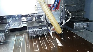
Photo 1. Final board routing.
In the case of small, light boards the void can draw it as trash or, even worse, move the already cut boards on the laminate thus causing scratches on the surface of the remaining circuits. In the case of v-cut scoring individual boards with sizes smaller than 30 mm, getting out of format becomes problematic. The separation process is also extremely time and money-consuming in such a case. If one of the dimensions is smaller than 5 mm, breaking without risking circuit damage is virtually impossible.
V-cut scored panel
Use of a v-cut scored panel constitutes the best solution for small circuits as it guarantees stability and easy separation in the future. V-cut scoring consists of cutting the laminate on both sides with disk blades. The produced grooves are located on board edges in the panel (Photo 2).
The standard unscored thickness i.e. allowing support for the circuits in the panel is 0.3-0.5 mm. A v-cut scored panel guarantees high rigidity, regardless of the number of boards. It does not necessitate use of any additional margins or frames unless this is necessary for other reasons (e.g. for assembly).
Photo 2. V-cut scored panel with margins (top and bottom side)
The maximum use of materials constitutes an undisputable advantage of v-cut scored panels. It is not necessary to use additional spaces between boards that would finally end up as waste.
This does not mean, however, that there are no limitations on using panels of this type. The basic condition for the exclusion of v-cut scoring is laminate thickness which needs to exceed 0.5 mm. Similarly, the quality of the circuit edge finish and dimension tolerance is smaller than for routing. Cutting disks only work in two directions: vertical and horizontal. Therefore, it is only possible to prepare panels with v-cut scored edges for rectangular circuits.
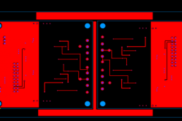
However, v-cut scoring requires the use of specific rules for preparing mosaics, as grooves determining circuit edges have a specific width. When designing the circuit, the correct distance between mosaic elements and the edges needs to be kept so that they do not get damaged during this process. Groove width and, as a consequence, maximum distance between the mosaic and the edges, depend on laminate thickness. For a standard laminate of 1.55 mm this distance is as much as 0.4 mm (Fig. 3), whereas for a routed edge it is only 0.15 mm.
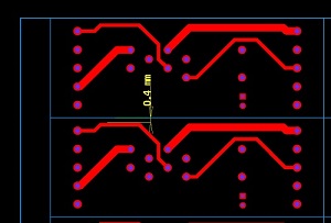
Fig. 3. Distance between path and v-cut scored edge.
V-cut scored panels cannot be used with thicker laminates unless the assembly specialist has a special panel or cutter separator. The unscored thickness for laminates exceeding 2.4 mm needs to be more than the standard 0.5 mm. This is because the panel can disintegrate in production under its own weight. This makes it impossible to manually separate the panel without the risk of circuit damage. Therefore, panels on thick laminate are routed.
Fully v-cut scored panels should be used for individual circuits with a size not smaller than 30 mm as it is virtually impossible to separate smaller circuits without special tools. Circuits of this kind should be produced in fully-routed panels or panels with mixed processing allowing for easier separation in the future.
Routed panel
Routed panels are used when it is impossible to use v-cut scoring.
They have bridges connecting boards with one another and/or with the panel frame. This type of panel is dedicated to circuits smaller than 30 mm regardless of shape, or larger circuits with irregular shapes (e.g. round, elliptical).
The construction of a routed panel necessitates the application of several rules. It is preferable to construct it with the smallest possible number of boards that would at the same time be large enough for the assembly process to be time-optimised. Together with an increase in the number of circuits in the panel, routing removes more and more material thus deteriorating stability. As a result, they can bend during production and assembly, or even break totally before they reach the recipient. To achieve the best possible panel rigidity, it is necessary to use an appropriate number of bridges supporting individual boards in the panel. It is assumed that a minimum of one bridge should be used for each 50 mm of circuit edge. A larger number of bridges is recommended for complex
shapes and thinner laminates. Designing only two bridges for only horizontal or only vertical edges (Fig. 4) constitutes incorrect practice. In such a faulty configuration of bridges for a large number of boards in a row, only connected along two edges, there is a danger that the panel will break apart in production.
(a)
(b)
Fig. 4. View on an non-stable panel (a) in which 2 bridges have been used for horizontal edges of the boards (b)
A thin fragment of laminate gives in much easier thus the final dimensions of individual boards are different than expected. Edges without a grip may prove uneven. However, there are situations in which an excessive number of bridges should be avoided. They increase the rigidity of the panel structure but at the same time they increase routing time and cost. This results from the fact that the number of times a route enters the material significantly influences the duration of the process and this in turn is directly influenced by the number of bridges used.
The rigidity of the panel and quality of circuit edges after depanelisation is also influenced by the type of bridge. We distinguish 3 types of bridges: without perforation, with perforation and v-cut scored.
Bridges without perforation (Photo 5a) are the best solution guaranteeing panel stability and edge quality after breaking the board away.
Separation is possible with just a routing machine. Bridges with perforation (Photo 5b) are the most popular as they provide optimum stability with relatively easy depanelisation. Disadvantages include break-away remnants protruding circuit contours and uneven edges in bridge areas (Photo 5c). This negative phenomenon can be attenuated by moving perforation holes to the inside of the circuit. However, an appropriate distance between perforation and the mosaics needs to be kept so that these do not get damaged by stress occurring when boards are broken away from the panel. V-cut scored bridges can only be used on horizontal and vertical edges. Ease of separation constitutes their main asset, but simultaneous routing and v-cut scoring the same edges unduly increases machining costs. Moreover, the laminate creates “hair” as a result which may impede the assembly process.
(a)
(b)
(c)
Photo 5. Routed bridges without perforation (a), with perforation (b), remnants after breaking boards away from the panel (c).
A routed panel should have an additional frame around the edges to increase the stability of the whole structure. Minimum thickness is 7 mm. In order to get such a frame, a laminate strip of 9 mm (from circuit edge to panel edge) is necessary. The 2 mm difference in thickness is intended for route passage. Typical frame width is 8-10 mm. The wider the frame, the greater the panel rigidity. Additionally, bridge perforation on the frame side is skipped for strengthening.
A standard route used by circuit manufacturers, including TS PCB Techn-Service S.A., has a diameter of 2 mm. Such should be the minimum distance between boards to guarantee optimum dimension tolerance and edge finish with the shortest routing time. It is possible to use smaller distances and, therefore, smaller routes. However, this will deteriorate panel rigidity and can lead to failure to keep the assumed dimensional tolerance of the circuit. Moreover, smaller routes require a reduction in the rate of feed which translates into prolongation of the process and increase in its price.
In order to increase panel rigidity, especially with small circuits, distance between the boards is increased on purpose to 9 mm (2 mm for tool and 5 mm of frame keeping the board). Usually, it is enough to keep greater distances between rows (Photo 6) and columns. In such a case, additional laminate strips together with the panel frame create a stable structure for individual boards allowing for the safe production, transport and assembly of circuits. Separating the circuits over smaller distances leads to the creation of a 1-2 mm wide frame, which significantly deteriorates panel rigidity.
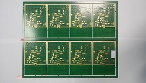
Photo 6. Stable routed panel with frame and a margin between boards.
A large surface of waste constitutes another disadvantage of processing with routing. When using distances between individual panels larger than 2 mm, waste amounts to as much as 50% of the whole panel surface. Routing is more expensive than v-cut scoring. However, it guarantees achievement of dimension tolerance at the level of as little as ±0.05 mm with CNC routing machines based on a mosaic. The v-cut scored edge forms a triangle in a cross-section, whereas the routed edge is smooth and straight without unnecessary remnants of laminate or plastic threads (Photo 7).
Photo 7. V-cut scored edge with visible laminate remnants.
Show more from category PCB documentation
-
PCB documentation

Integr8tor - problems solving
-
PCB documentation

Integr8tor—project processing
-
PCB documentation

Automated Analysis of PCB Designs - the process of creating production documentation
-
PCB documentation
How to optimize machining of printed circuits? - part 1
-
PCB documentation

Bridges – structure and parameters
-
PCB documentation

What to remember while designing multilayer PCBs?
-
PCB documentation
Accepted file format for printed circuit board designs
-
PCB documentation
How to correctly design panels for small circuits? - part 2
-
PCB documentation
Proper preparation of copper layer
-
PCB documentation
Proper preparation of solder mask layer
-
PCB documentation

Proper preparation of PCB outline
-
PCB documentation
PCBs production documentation – how is it created and what are its contents?