How to correctly design panels for small circuits? - part 2
17.05.2017
.png)
Routed and v-cut scored panels
Each circuit form, unless rectangular, necessitates routing. V-cut scoring is necessary if circuits in the panel have at least one vertical or horizontal edge; in such a case it will be possible to route the remaining edges.
Mixed processing (Photo 1) allows one to reduce the disadvantages of both methods used separately. It is also recommended for rectangular circuits smaller than 30 mm as it facilitates separation of boards when compared to a fully v-cut scored panel.
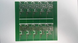
Photo 1. Routed panel (horizontal edges and cuts) and v-cut scored panel (vertical edges) with frame between two rows of boards and on vertical edges.
Circuit edges parallel to panel edges need to be v-cut scored. It provides a more secure grip over a longer length than in the case of an individual perforated bridge with standard length of 2 mm.
Slant edges, arches and cuts in the circuit interior need to be routed.
Mixed panel processing necessitates the application of a frame around the circuits. For a v-cut scored edge, 5 mm is enough and therefore the unused laminate surface is significantly smaller than in the case of fully routed panels.
Mixed processing is sometimes used for rectangular boards with mosaics placed too close to specific edges. They are then routed as it allows for the placing of mosaic elements significantly closer to the edges. Use of v-cut scoring for some edges allows a reduction in both time and cost of machining.
Distribution of copper in the panel
The distribution of copper constitutes an equally important issue in designing panels.
A uniform and symmetrical percentage of copper surface per square centimetre of circuit is the most desirable. It is crucial during the production of circuits. It is of special importance at stages during which laminate is subjected to high temperatures. Uneven distribution of copper may cause board distortion and future difficulties in assembly as a consequence (Fig. 2).
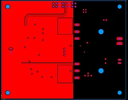
Fig. 2. Board with uneven copper distribution
Moreover, circuits with metallised openings subjected to electroplating may exhibit excessive thickness of paths and pads in areas with significantly less copper in relation to the whole circuit surface. This in turn may cause incorrect covering with antisoldering mask thus increasing the risk of short-circuits during assembly.
In order to avoid problems of this kind, placing boards with very different distributions of copper in a single panel should be avoided. When constructing such a panel, copper balance may be compensated with the addition of a lattice or mosaic rectangles that would “protect” the areas at risk of copper overgrowth. It may prove equally efficient to place boards in the panel in such a way that they are turned in relation to each other by 180 degrees. Please note that areas with larger copper density should be closer to the external edge of the panel. Application of both techniques of copper distribution symmetrisation has been shown in Photo 3.
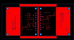
Fig. 3. Panel with board with uneven distribution of copper with added filling in the frame
Summary
The two sections of the article discuss various methods of the mechanical processing of panels with regard to producing small circuits. Characteristics and methods for increasing mechanical stability have been presented for both of them. Moreover, elements allowing for reduction in panel production costs while keeping their mechanical strength have been discussed. Guidelines for engineers and designers have been discussed and issues to be avoided in constructing panels have been mentioned.