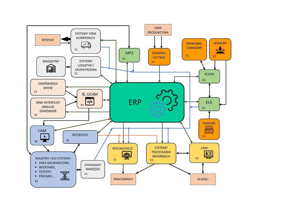
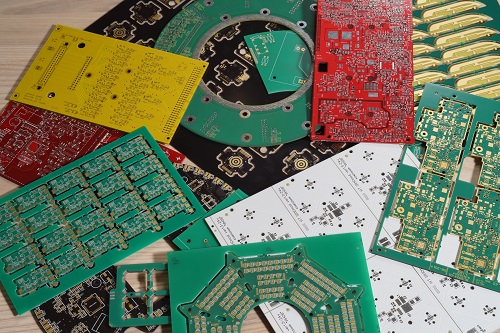
PCBs production documentation – how is it created and what are its contents?
08.02.2016
While designing a printed circuit board, the designer develops a vision of a printed circuit of which the connection network will ensure its correct and faultless operation. This vision is reflected in the electronic version of the design, prepared in a CAD program, and the design documentation generated for the printed circuit manufacturer. On its basis, the proper production documentation is created to be used at the particular stages of circuit production. It includes, for example, films for reproducing the particular circuit layers (mosaics, soldermasks, silkscreens), programs for mechanical treatment (drilling, milling and scoring) for CNC machines and programs for optical and electrical testing.
The article explains the process of preparing production documentation following the sequence of the particular stages of production, at which it is used.
For a better illustration of some production processes, more detailed descriptions are included.
Design and manufacture technology
As the widespread standard of design documentation storage, the Gerber RS274-X and ODB++ formats are accepted by most renowned PCB manufacturers. Currently, there is a great variety of CAD software that support developing circuit designs available on the market. Most programs, including the most popular ones (Altium Designer, Protel, Eagle), support exporting data in these formats.
The design documentation must be full and cannot cause difficulties in the understanding of the designer's expectations. Correct understanding is facilitated by maintaining a clear and concise nomenclature of files and by deleting any sets that are unrelated to circuit production, for example sets of files dedicated to assembly. Apart from the design files, the documentation must include the specification of the circuit manufacture technology. This is an essential part of the production documentation, which defines: the materials required for the production, the sequence of technological processes and their parameters. Seemingly insignificant lapses in the entries on technology, for example excessively general or missing information, may result in the production of circuits that do not meet the original assumptions of the designer. Only a few technology parameters can be corrected during or after production, therefore very few manufacturers, including TS PCB, allow allow to implement corrections. Unfortunately, in most cases the consequences of an incorrect specification of the design technology are irreversible.
CAM processing
The initial stage that precedes production is the verification of feasibility of the printed circuit board and its adaptation to the requirements and process parameters. The implementation of the design modifications suggested by the PCB manufacturer ultimately enables obtaining a high quality and reliable circuit in accordance with the designer's concept and the IPC standards. Usually, the proposed changes relate to:
- maintaining the minimum distance between the copper and the edge to ensure suitable electrical insulation and to prevent damage during machining,
- enlarging the rings around holes or adding teardrops to protect connection continuity at the via-path boundary,
- enlarging paths by the etching coefficient to ensure their suitable width,
- selecting correct exposure sizes in the soldermask to prevent it from overlapping the pads,
- correcting hole diameters to make them with an appropriate tolerance,
- thickening the silkscreen lines to the minimum values and cutting the lines extending onto the pads and exceeding the board silkscreen.
In the professional manufacture of circuit boards, the so-called production formats are used, which are large laminate boards of a standardised size, adjusted to the complete technological sequence. While preparing for the production, the CAM engineer uses the available working area of the format to place the particular layers of a single circuit or panel to ensure the optimum use of its surface. Next, in the format frames, outside the working area, base holes and other marks are placed to enable the correct installation of formats in the individual machines of the production line. This approach facilitates production and increases its efficiency and repeatability.
Reproduction of conductive layers
The primary component of the production documentation are conductive layer films. The method of photo-chemical subtractive etching of unnecessary copper surfaces is commonly used for the reproduction of connection mosaics. For this purpose, a photosensitive substance (photopolymer) is applied onto the laminate, which is initially entirely coated with copper, and its selected areas are UV-cured in an imager. To prevent accidental imaging, the process takes place in rooms where light sources do not emit radiation of this range. Furthermore, to maintain the high-quality of mosaic reproduction, a very high level of cleanliness is maintained and air humidity and temperature are monitored on an ongoing basis.
In the classical method of imaging of the outer layers of copper, positive films printed and developed on a photoplotter are used, in which the mosaic is reproduced using its black elements. Later, the films and polymer-coated production formats are inserted into the imager that enables simultaneous imaging of both sides (top and bottom). The copper under the cured areas is removed in the further etching process. However, the inner layers and one-sided circuits are imaged with negative films due to the omission of the metal-coating process.
To achieve the most precise geometrical layout of the mosaics in the film in relation to the production format, special systems of reference positioning and imaging are used. Renowned PCB manufacturers, including TS PCB, use highly advanced imaging systems. One of them is the OLEC system that ensures automatic reference positioning according to the reference points placed in the film and the production format (fig. 1).

Fig. 1. OLEC imager – preparing for exposure.
Another advantage of the OLEC system is perpendicular UV ray alignment in relation to the entire laminate surface, due to which the imaging precision is very high and the problems typical of the legacy systems, resulting from the variable imaging angles and resulting in polymer backlighting, no longer occur.
The newest generation machines support direct imaging of the photopolymer, while omitting the films. An example of this type of imagers available on the market is LEDIA and one of 18 specimens of this machine manufactured worldwide works with TS PCB. An essential advantage of this technology is plotting (imaging) images in a variable scale, adjusted on an ongoing basis to the production format size, which eliminates laminate deformation and ensures perfect alignment between the mosaic and the drilling.
Soldermask and silkscreen layers
At the following stages of production, soldermasks and component silkscreen layers are applied onto the etched surfaces of production formats, made with special thermosetting photo-sensitive paint. Soldermasks are made using two methods: the curtain method (so-called photo-mask) and the screen-printing method. In the curtain method, the production format passes through a wide flow (waterfall) of paint (fig. 2), which coats it entirely.

Fig. 2. Production format (at the bottom) passing through a mask curtain (at the top).
Initial curing of the applied layer takes place at an increased temperature and protects the surface from mechanical damage during the following operations. The curtain method is very efficient and precise, and it enables maintaining very high laminate surface purity. Unfortunately, a single curtain application line can use only one paint type and soldermask colour (green being the most popular) and its refitting is very troublesome.
The screen-printing method offers a wider range of paint types and colours, and does not require an expensive machinery stock. Also in this case the soldermask is applied onto the entire production format, but this time through a special screen which reproduces the layout of soldering points. This method is more time-consuming and achieving the equivalent mask image parameters is more difficult in relation to the curtain method.
For silkscreen layers, there are two methods of application: photo-printing, which consists in applying the paint onto the entire format and imaging selected areas, and screen-printing, in which the silkscreen paint is applied selectively onto the selected areas, followed by curing. The first method allows obtaining high resolution image at the cost of higher material and film consumption. It is used mainly for smaller surface designs and when the highest quality of silkscreen layers is required.
The imaging of the photo-masks and photo-descriptions takes place analogically to the imaging of mosaics with films. Because it requires significantly higher imaging power than for the photopolymer (mainly due to the thickness), using the direct imaging method in this area results in technical difficulties in the manufacture. If the LEDIA system was used for this purpose, the supply of the necessary imaging energy would take too much time (single minutes). An interesting alternative to silkscreen layer application using screen-printing may be the use of an automatic printer, which in its operation is similar to a traditional computer inkjet printer.
Machining
Typical production documentation includes a set of files for CNC machines which describe mechanical treatment, most frequently milling. A widespread format of files dedicated to machining is Excellon (currently in version no. 2), which is used to control CNC machines directly. A correct file must include the definitions of tool diameters, which may be placed in its header or a separate file. One must remember that the PCB manufacturers understand the indicated tool sizes as target whole diameters or slot sizes, unless stated otherwise in the technological specification. The file header should also contain additional information on the unit (mm, inches), scale and the omitted set of leading or trailing zeros. Drilling and milling may be also entered in the Gerber format, which has certain advantages – it eliminates the problem of centricity and precision of mechanical layers in relation to other layers.
For designs with varied machining, separate files should be generated and properly described for each operation. This will reduce the risk of misunderstanding of the designer's concepts. One should also remember that each machining operation may be performed differently, which results in individual and typical process limitations that influence its feasibility for the design.
The production documentation includes additional necessary commands, definitions, and modified tool diameters, which enable the achievement of the dimensions specified in the project. It is essential in particular for metal-coated holes and sockets, for which an additional layer of galvanic copper and finish coating (tin plating, gold plating) should be considered. Normally, tool diameters for such holes are incremented by 0.1 mm to ultimately obtain the hole diameter expected by the designer, while maintaining the typical tolerance of +0.1 mm / -0.05 mm.
Outside the standard drilling and milling program, the design documentation may also include scoring and phasing programs with the depth and co-ordinates of scoring lines. In most cases, neither the scoring nor milling is specified for the design directly using dedicated files, but as machining layers with a silkscreen and lines separating the particular circuits, for example in a panel. Unfortunately, sometimes it causes misunderstandings, resulting in the omission of some machining operations, when circuits are manufactured.
Testing
The production documentation also includes optical and electrical testing programs. The manufacturers of high quality circuit boards, including TS PCB, perform an optical inspection of the AOI circuits that are used to check the mosaics after the etching process. This consists in comparing the scanned real image of the circuit with the image generated based on the original design documentation. This way, any deviations in the manufactured circuit image are verified and it is determined whether they follow the acceptable tolerance. The inspection of AIO circuits is an internal test, performed regardless of customer requirements.
a) 
b) 
Fig. 3. Testers of circuit boards: a) finger tester, b) adapter tester.
Due to the increasing complexity of circuit boards, electrical testing is necessary apart from the optical testing. Analogically to AOI, the test program is created independently on the documentation prepared by the CAM engineers, based on the original design files. Thus, the connection network of the manufactured circuit is compared to reference, which enables finding the faults that arose in the production.
In most cases, electrical testing is performed using two methods: the Flying Probe method, sometimes referred to as the finger test (fig. 3a) and the Bed Of Nails, also referred to as the adapter test (fig. 3b). The first method consists in measuring the continuity and capacity of the networks being tested using mobile probes that enable the measurements to be performed on both sides of the printed circuit, which allows the testing of the most advanced HDI circuits and circuits in production forms. Adapter testers have a smaller working area and a limited resolution of placement of testing needles and assembly plugs. The manufacture of an adapter suitable for the given design is a time-consuming process. However, their essential advantage is the unique short testing time of single seconds per circuit or panel.
Conclusion
The article presents the process of preparing production documentation for circuit boards based on the design documentation supplied by the customer. Therefore, correct preparation of the design documentation is essential to the manufacture process and to ensuring the highest reliability and quality of circuits. Thus, one should be particularly careful when formulating technological requirements and the boards should be designed according to the commonly used standards and requirements of the PCB manufacturers.