
Proper preparation of PCB outline
Łukasz Romik Author
A common mistake in printed circuit board documentation is an incorrectly prepared outline layer.
A properly prepared outline is shown in Fig. 1 – the line with constant width clearly indicating the printed circuit perimeter edge. Fig. 2 additionally shows it paired with a mosaic layer.

Fig. 1. Correct printed circuit boards outline (through-holes are also visible).
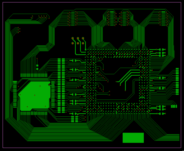
Fig. 2. Correct printed circuit board outline paired with mosaic layer (through-holes are also visible).
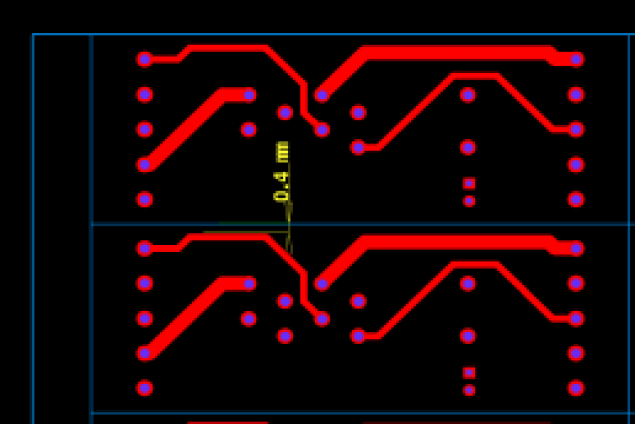
Setting an outline layer so prepared on the project’s remaining layers (mosaic, silkscreen, etc.) usually does not cause major problems. However it may happen that, for example, some mosaic components stick to the edge (usually a certain distance should be kept) and when the outline is set on the mosaic, a short circuit develops (Fig. 3). It may seem that removing the outline lines will not cause a problem, but it should be kept in mind that this is a manual operation, prone to mistakes.
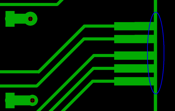
Fig. 3. Outline line with pads sticking to the edge.
It also happens that an outline marking layer comprises further components (e.g. assembly tags, component outlines etc.) that should not be there (Fig. 4 and Fig. 5).
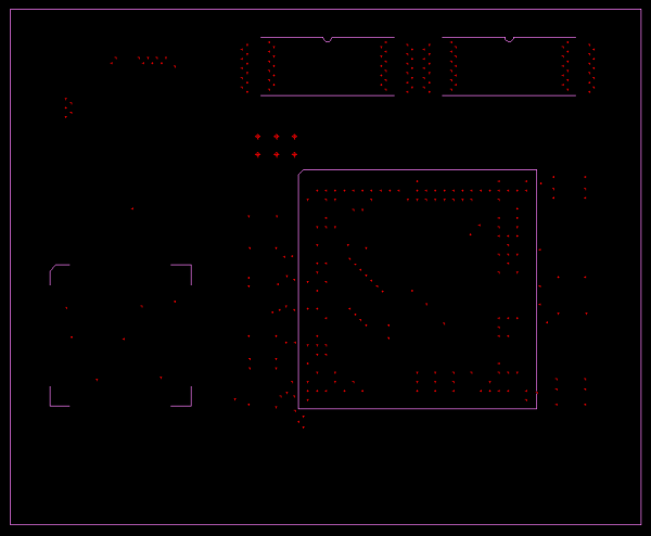
Fig. 4. PCB outline layer with unwanted component outlines inside.

Fig. 5. PCB outline layer with unwanted component outlines inside – paired with a copper layer.
Setting such a layer on, for example, a mosaic (Fig. 6) can lead to the problem shown in Fig. 7.
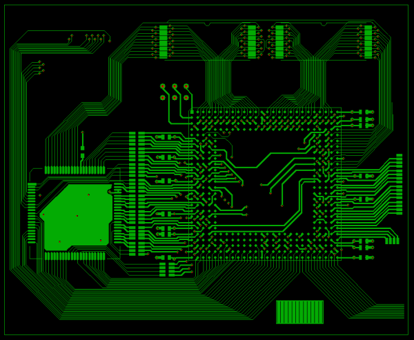
Fig. 6. PCB outline layer with unwanted component outlines inside, set on a copper layer.
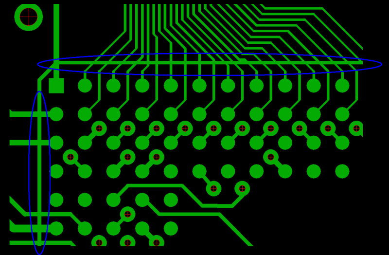
Fig. 7. Outline layer components that cause short circuits in the mosaic.
In order to to safeguard against these problems, the PCB outline should be set on a separate mechanical layer, e.g. GM1. It may also contain internal milling and scoring lines. However, if we want to provide a documentation, which is likely, it is worth moving the milling and scoring to separate layers. Lines, tags and lettering which do not belong to the PCB outline should be moved to a separate mechanical layer.
Show more from category PCB documentation
-
PCB documentation

Integr8tor - problems solving
-
PCB documentation

Integr8tor—project processing
-
PCB documentation

Automated Analysis of PCB Designs - the process of creating production documentation
-
PCB documentation
How to optimize machining of printed circuits? - part 1
-
PCB documentation
Bridges – structure and parameters
-
PCB documentation

What to remember while designing multilayer PCBs?
-
PCB documentation
Accepted file format for printed circuit board designs
-
PCB documentation
How to correctly design panels for small circuits? - part 2
-
PCB documentation
How to correctly design panels for small circuits? - part 1
-
PCB documentation
Proper preparation of copper layer
-
PCB documentation
Proper preparation of solder mask layer
-
PCB documentation
PCBs production documentation – how is it created and what are its contents?