Proper preparation of solder mask layer
30.11.2016
A common mistake in printed circuit board documentation is an incorrectly prepared solder mask layer.
Its correct implementation make it possible to eliminate problems at the PCB production stage and also in the process of component installation in circuits. It is inappropriate to prepare the mask layers flush with a pad to be exposed. The situation whereby there are exposures in customer sets that expose the mass or are very close is also unacceptable.
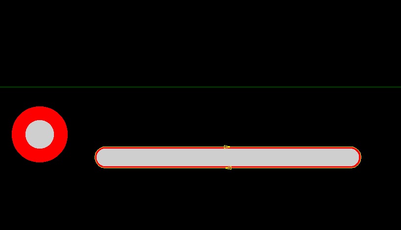
All components to be tinned or gilded must be exposed by a mask enlarged by at least 6 mils in relation to the component in the mosaic. In other words – the minimum exposure on the mask is 3 mils on each side of the component, as shown in Fig. 1.
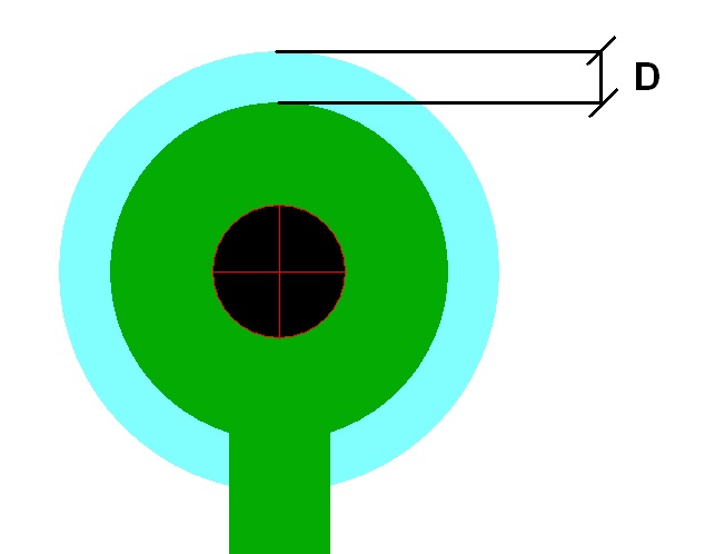
Fig.1. Pad exposure on mask – D minimum exposure per side.
It is very important that the solder mask is properly prepared for integrated circuits in QFP, SOJ, etc. type enclosures. For such circuits it is important to determine whether the solder barrier between the individual pads of these circuits is necessary. The minimum width of this barrier is determined by the circuit supplier. Example parameters for TS PCB manufacturer are shown in Fig. 2.
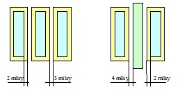
Fig.2. Distances between components on mask for QFP circuits.
Fig. 3 presents the properly prepared exposures where the solder barrier is applied. Its width meets the requirements of TS PCB manufacturer's processing capabilities and the minimum exposures for mosaic images alike.
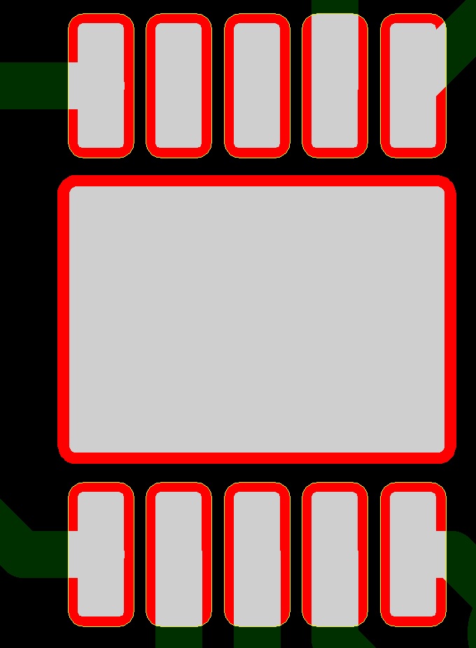
Figure 3. Properly prepared exposures with solder barrier for integrated circuits.
Where no solder barrier between the chip's pads is absolutely necessary, the exposure preparation should look like in Fig. 4. In this case, the space between the pads has been exposed and there is no solder mask between them.
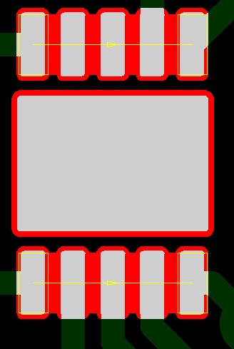
Fig. 4. Properly prepared exposures without solder barrier for integrated circuits.
Solder mask preparation for circuits in BGA and uBGA enclosures
Due to the fact that BGA and uBGA circuit board pins are set under them, it poses many hazards in printed circuit manufacture and component installation on the board. One of the biggest threats is unmasking the vias and tracks adjacent to solder points, which after the circuit's assembly may cause short circuits. After assembly, this kind of circuit is virtually unrecoverable, so vias in the BGA area must be masked.
If there is an uBGA circuit on a board (pads spaced by not more than 0.8 mm), exposures absolutely must be applied to the mask by 2 mils per side.
If there is a BGA circuit on a board (pads spaced by more than 0.8 mm), 2 mils exposures should be applied, or 3 mils where possible.
Fig. 5 presents the properly prepared exposures for BGA circuit boards. Vias under the circuit board are covered with a mask and only the pads under solder balls are exposed. In this case, there should be no problem during component installation resulting from an incorrectly prepared solder mask layer.
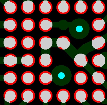
Fig. 5. Properly prepared exposures for BGA circuit board
Preparation of masks for plated holes
All plated holes should be fully exposed or covered with a solder mask, because no hole can be made partly exposed / covered.
A properly prepared exposure under a plated hole is shown in Fig. 6.
Fig. 6. Properly prepared exposure under plated hole