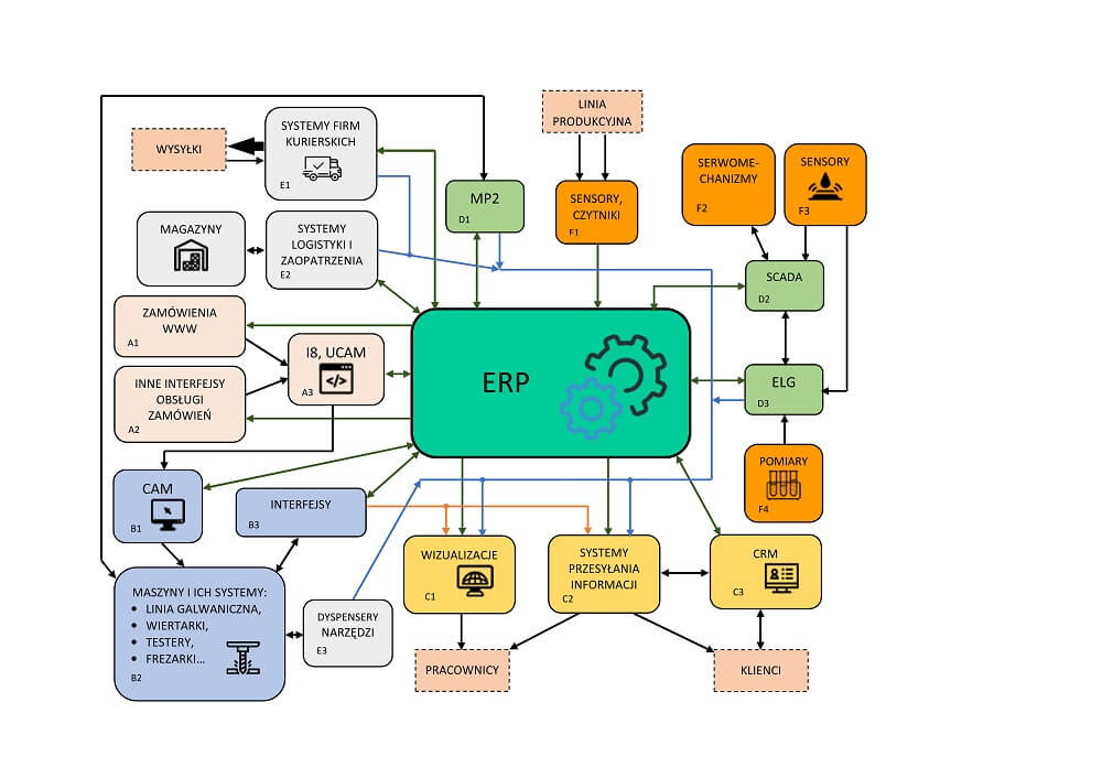
Manufacture of printed circuits in harmony with the natural environment - recycling
One of the ways to minimise the impact on the natural environment is the reuse of materials recovered from waste accompanying PCB manufacture. This technique reduces the final amount of waste and the use of natural resources. A list of the main waste groups (or their components), together with the processes in which they arise and types of recovered raw materials are presented in Table 1. Some recyclable waste is described in more detail below.
|
Waste name |
Process |
Recovered raw materials |
|
Dross from tin welds |
Tinning |
Tin, copper |
|
Laminate offcuts/leftovers |
Mechanical treatment |
Gold, tin, copper, nickel |
|
Remains of copper foil |
Ironing |
Copper |
|
Worn drills, milling cutters, saws |
Mechanical treatment |
Steel |
|
Aluminium sheet |
Mechanical treatment |
Aluminium |
|
Used photographic plates |
Photoengraving |
Silver, developer |
|
Used gilding bath |
Gilding |
Gold |
|
Waste baths from the processes |
Copper etching, etching... |
New baths |
|
Mixed packaging waste |
Auxiliary processes |
Plastics, cellulose |
Table 1. Waste subject to recycling.
Tinning is the most popular method for the final coating of printed circuits. It is usually carried out using the HAL (or HASL) method, in which the circuits are immersed in a lead-free tin alloy with a temperature of approx. 280°C. The bath is gradually contaminated with copper, impairing the working parameters, and therefore it must be cleaned periodically. For this purpose, the temperature of the alloy is lowered by approx. 50°C, allowing the impurities (copper and fluxes) to crystallize at the bottom of the tin bath. Pollutants - dross from tin welds (Photo 1) - is then mechanically removed.
%20small.jpg)
Photo 1. Dross from the tinning process.
Printed circuits are manufactured on large laminate formats, with specified sizes, to which the entire technological line is adapted. One of the final stages of manufacture is machining, the main purpose of which is to extract circuits from panels. The remaining laminate is referred to as offcuts. Sometimes they include defective circuits, rejected during the manufacturing process, as well as defective panels unsuitable for further manufacture. Due to various metals being recycled, tinned and gilded offcuts are collected separately (Photo 2).

Photo 2. Segregation of laminate offcuts.
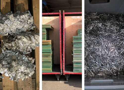
Another waste generated during machining constitutes used drills, milling cutters (Photo 3) and saws that cannot be reused. In the case of drills, their lifetime is determined by the number of holes drilled, and wear manifests itself in becoming dull. In order to limit the number of drill bits scrapped, a lot of which is used up during drilling while maintaining high quality of drilling, some of them are re-sharpened.
%20small.jpg)
Photo 3. Worn drills and cutters.
Another type of waste generated during machining is aluminium sheet occurring in two forms: as offcuts of PCB panels with aluminium core and as a thin sheet (Photo 4) used during drilling, among others to stabilise drills and remove heat. Aluminium sheet in both forms is handed over for scrapping.
%20small(1).jpg)
Photo 4. Aluminium sheets after drilling.