
PCB quality depends on designers
Łukasz Romik Author
The quality of printed circuit boards (PCBs) relies heavily on the design method. It is the stage at which the designers already define the production workflow and the probability of quality defects. Many potential errors can be avoided by introducing cosmetic changes to the design, which will provide better quality of the finished product. The following showcases a slew of hits for PCB manufacturers on how to build the boards and keep their quality high.
The process of PCB design should consider the electrical parameters of the PCBs along with the production capacities of the supplier selected to deliver the purchase order. PCB manufacturers specify the principles they require to follow in the design to make the boards manufacturable. The usual recommendations include, among others:
- The minimum spacing of conductive parts;
- The minimum path width;
- The minimum hole diameter and ring sizes;
- The minimum solder mask exposure;
- The number of layers, etc.
It is necessary to analyse each design for these factors in order to deliver a good PCB. However, all deviations from the stated principles are easy to detect, since most modern PCB design systems feature design checks and error correction measures.
The solution to the right is good: the paths with the minimum permitted width have been widened, and thus the risk of overetching and mechanical damage is largely reduced.
In-production problems arise more than often as caused by the design solutions, while the processing principles have been followed to the letter. This is what can reduce the PCB quality. This article will follow with a discussion of how to eliminate these problems.
Copper and path surfaces
One of the predominant problems is the incorrect distribution of the copper surface on the outer layers. The effectiveness of electrochemical copper deposition on the PCB surface and hole interior strictly depends on the homogeneity of copper distribution across the PCB surface.
The PCB parts with low component density (i.e. singular insulated paths and holes) will have higher copper fill levels than other parts of the product that feature denser packing or large copper areas.
These solutions make it hard to comply with the designed hole diameter tolerance or proper solder resist deposition of excessively thick paths in high density areas. The copper spread can be improved by adding an extra copper area in low density parts. The extra copper will have no electrical function, it will only help properly distribute the copper in electrochemical metallization.
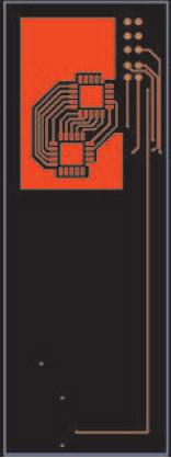
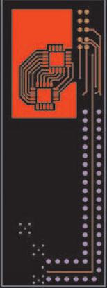
Fig. 1. This solution is not recommended and must be avoided. The solution to the right is good: the insulated paths and holes are protected with extra copper fills.
Fig. 1 shows a PCB before and after addition of special copper fills. Another problem is too long minimum width paths. Single insulated paths with the minimum permissible width cause trouble during PCB etching.
The paths can be easily overetched and are also exposed to risks of mechanical damage and open circuit formation. A good design rule is to reduce the minimum width path length. This is done, for example, by leading a 4 mils path in heavily dense areas and increasing the width by 2-3 mils in less dense portions of the PCB, see the example in Fig. 2.
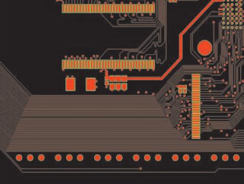
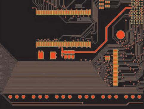
Fig. 2. This solution is wrong. The two bottom paths are exposed to overetching and can be easily damaged.
Pad beads
More than once have quality problems with PCBs arisen from the lack of beads at small pads (rings). A drilled hole may be tangent with a pad edge. The solution is permitted, but not when the hole touches the pad edge at the path and pad joint.
Then the risk of an open circuit increases by leaps and bounds. A bead is added to the pad in this case. The bead should overlap the path by a minimum of 5 mils. This principle is crucial, especially for small hole diameters (0.3 mm or less) and when minimum permissible rings are used, where the probability of hole non-centricity is increased due to the insufficient stiffness of the drill bits.
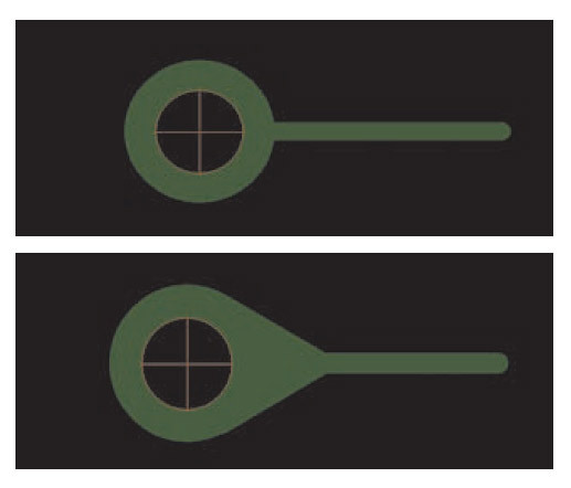
Fig. 3. Bad solution for minimum permissible rings, and a good solution with an extra bead.
Fig. 3 shows the recommended solution. Production defects and quality problems of finished PCBs are also caused when the design leaves a free space less than 5 mils wide between a pad and a path.
Once the photopolymer is exposed and developed, a strip of the material that is 5 mils wide or smaller has a limited adhesion. This very often results in detachment and sticking of the piece to another part of the PCB. This causes open circuits or shorting, depending on the PCB technology. Fig. 4 shows the problem, and Fig. 5 shows the recommended solutions.
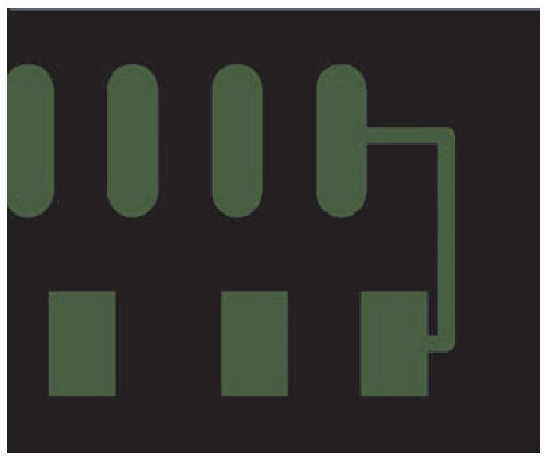
Fig. 4. The clearance between the bottom pad and the path is too small.
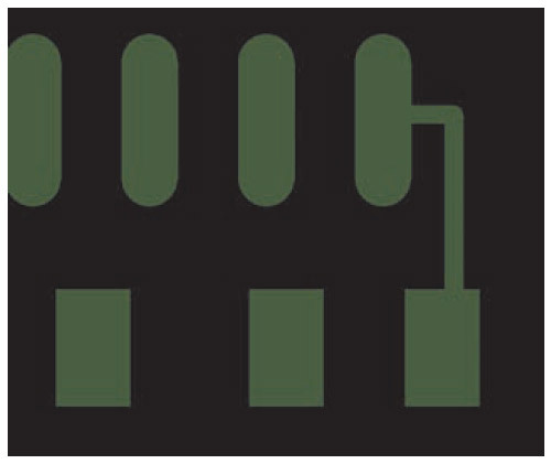
Fig. 5. The solution is good: correct clearance between the pad and the pad.
Spacing
Another cause of problems may consist in leaving solder mask (resist) areas that are less than 3 mils wide. Solder mask areas less than 3 mils wide have reduced adhesion and tend to chip, not unlike the photopolymers. This is especially evident in ENIG processed PCB, where the bath effect is aggressive to the mask.
The areas must the wider or completely removed from the design. Small copper residues on PCBs are also problematic. The PCB design must include a solution that will not leave small, obsolete parts of copper on the surfaces.
Small copper residues adhere poorly to the laminate, and when they do break away during the resist deposition, the predominant effect is shorting. Fig. 6 shows this problem. PCB quality can also be affected by high differences in the copper surface area between the top and bottom surfaces.
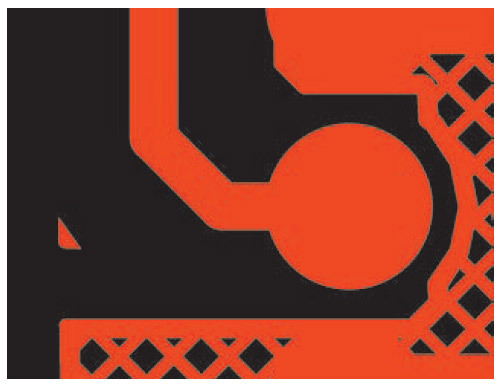
Fig. 6. Inadvertently applied copper.
This causes mechanical stress. Consequently, such PCB design tend to bend during thermal processing. This occurs especially in PCBs that are less than 1.5 mm thick. If possible, it is recommended to apply a complementary copper filling on the PCB side with the smaller copper area, or install a copper mesh on the large copper surface side.
The solution removes the stress and the risk of PCB deformation. Fig. 7 shows a copper mask that replaces compounds with full copper surface. When building a mesh you need to remember that the square mesh size must be at least 8 mils long and the mesh line must be at least 10 mils thick. The last problem on the list is the production of large surfaces without copper on the inner layers.
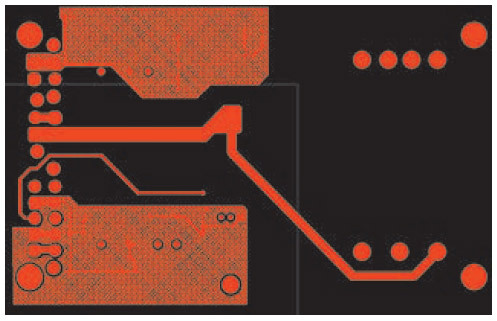
Fig. 7. A copper mask replaces compounds with full copper surface.
Fig. 8. This solution is not recommended: the black space on the PCB is a low pressure area. The solution to the right is good: the blank has been filled with copper.
The areas form the so-called ‘low pressure areas’ during the PCB pressing process. They require a lot of resin to be completely filled. If there is too little resin, empty blisters are formed that resemble delamination effects. A solution here is to add a non-functional copper area, as shown in Fig. 8. This rule is especially important when the copper thickness is ≥ 70 μm.
Surface usage
PCB designers can also define the finished PCB price by applying design solutions that may change the laminate surface usage. PCBs are not manufactured as one-off items. There are production formats applied (e.g. 460×610 mm), and PCB manufacturers recommend that the customers contact them when composing the PCB in panels to determine the optimum panel size which serves to optimise the consumption of materials.
Adding or removing just one PCB to or from the panel may often reduce the production waste from the laminate. These problems are usually a result of the mechanical, physical and chemical properties of materials and processes in PCB production.
All my hints favour enhancement of the processing window applied by PCB manufacturers. Hence a PCB prepared according to these proposed principles and rules will always be easier to build, and hence its production is faster, better cheaper and free of quality defects.
Show more from category Quality
-
Quality

Manufacture of printed circuits in harmony with the natural environment - environmental solutions
-
Quality

Manufacture of printed circuits in harmony with the natural environment - recycling
-
Quality

Manufacture of printed circuits in harmony with the natural environment - legal requirements
-
Quality
Manufacture of printed circuits in harmony with the natural environment - waste classification, storage and disposal
-
Quality

Testing printed circuits: AOI optical testing
-
Quality

Testing printed circuits: Blade testers
-
Quality

Testing printed circuits: Finger testing – testing time optimization
-
Quality

Testing printed circuits: Electrical testing – testers with moving probes
-
Quality

Testing printed circuits: Classification of the circuits testing methods and introduction to electrical testing
-
Quality

Base material of printed circuit boards: a few words about laminates
-
Quality

Certificate ISO 9001:2015 and 14001:2015
-
Quality

IPC circuit classes