Quality of printed circuit boards. Basic principles of evaluation
25.11.2015
 comments (2)
.jpg)
The current requirements and expectations of customers in the PCB sector for reliable and failure-free performance of purchased equipment are definitely higher than only a few years ago. An undisputed reason is the dynamic growth of technology with the concomitant progress in quality. Even the simplest electronic devices are expected to perform consistently and without fail for as long as possible. IPC 600 is a standard widely applied in the PCB industry to specify the quality of PCBs. This article shows the most important criteria of PCB reliability, which can be visually examined by PCB customers and which prove the finished quality level. The article highlights the features compliance with largely affects trouble-free assembly and failure-free equipment performance.
The basic evaluation of PCB quality is possible by reviewing the documentation provided by PCB manufacturers and thorough visual inspection of circuit surfaces. Those documents may include: proofs of compliance with purchase order, electrical testing reports, or certificates of compliance to special standards (e.g. IPC 600). The UL non-flammability certification may also attest a high quality of PCBs.
PBC manufacturers may, on customer's special request, make microsections, which is a destructive microscopic examination of quality of the deposited coats, and provide the analytic results in a report complete with the test sample. Microsections can be prepared from any part of the PCB specified by the customer, e.g. a specific via hole.
Some customers expect the PCB production to follow the Production Part Approval Process (PPAP). In this case a special documentation is made with master samples that are at the disposal of the PCB manufacturer and PCB purchaser. There are few manufacturers, including TS PCB, who offer the full delivery of all those documents with the ordered PCBs.
Visual examination of PCB surfaces allows detection of processing defects and typically 'cosmetic' flaws. The IPC 600 methodology requires visual inspection with a small magnification, which is usually ca. 1.75×. If the suspected defects are not visible, the inspection shall be with higher magnification values (up to 40×).
What to inspect
The first stage of the visual inspection may consists in checking the characteristic dimensions of the PCB. All dimensions (hole diameters, milled forms, etc.) must meet the design documentation requirements, especially when press-fit and Z-routing processes are applied. The next stage should verify the bending and twisting of the PCB.
Surface-mount PCBs must never have the bending and twisting of more than 0.75%; in all other technologies a limit of 1.5% applies. It is extremely critical that the PCB surface must be free of contaminants downstream the machining. Dust, particulates and laminate swarf are not permitted. The contaminants may cross-contaminate the solder. The pads must be free of fingerprints.
The PCB edges must be smooth, even and free of nicks, burrs or fuzz. The metallic coating of plated edges must be continuous and with proper adhesion strength. This verification is greatly enhanced with the tape peel-off test (ref. IPC-TM-650 clause 2.4.1). Scoring (v-cutting) must be thoroughly complete and deep enough to enable easy depanelizing and yet strong enough to prevent the panel from breaking under the load of assembled components. Multilayer PCBs must be free of fine cracking that is evident by white stains or characteristic criss-cross patterns visible under the base material. Separation of layers or localised swelling and delamination of the base structure is partial to poor quality of the PCB.
Another parameter of control is the quality of the solder mask (resist) layer. The layer must be uniform in appearance and free of scratches. Discolouration or filmy spots may indicate insufficient resist layer thickness and/or excessive thickness of the plating. The resist layer can be slightly offset, but not over the pads, test points, or inside of assembly PTH's. The rings around the holes must not be reduced. All details designed to be masked must be fully covered with the resist.
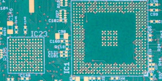
Image 1. PCB with a properly applied solder mask around the BGA's and a centric hole.
Adjacent electrically insulated conductors must not be exposed. Blisters, bulging, delamination or entrapment of contaminants in the solder mask is unacceptable. The entire resists must firmly meet the substrate. A critical parameter is the levelling of mask deposition and solder mask continuity over the surface-mount areas of BGA's. The solder mask must never enter the BGA pads or feature losses (see Image 1).
Requirements for solder masks and text layers
IPC 600 permits reworking of the solder mask/resist (provided that rework materials conform to the original mask parameters of resistance to soldering and cleaning); however, many reworks will be damaging to the perceived quality of the finished PCBs. The via holes to be filled with the solder mask must be filled. PCBs must not be contaminated with other coats, e.g. peelable masks or carbon compounds.
The text layer must be legible and complete. The ink may extend beyond the character line, or a part of the component outline symbol can be missing, provided that the mark remains well defined and legible. The ink must never enter the printed edge contacts or test points. The PCB parts visible in the finished device must have a perfect quality of the text and mask layer (see Image 2).
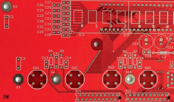
Image 2. Detail of a PCB with a good text layer built.
Reliability of equipment heavily depends on the metallization quality. It is also critical to keep the width and spacing of mosaic details in line with the design documentation. Coarse edges of mosaic components are permitted in IPC 600, but may harm the production quality image.
Albeit very difficult to visually examine, extremely tell-tale quality indicators include all sorts of lumps and burrs on or in PTH walls, metallization gaps or discontinuous cracks. If those defects are suspected, microsection testing is recommended. The holes may not be perfectly alignment with the pads, and ring breaches of less than 90° are permitted, but no hole can be located at the conductor to pad joint. Inspection of multilayer PCBs can be improved against a visible light background. This helps inspecting the arrangement alignment of the layers and the centricity of bores.
Coats are very tell-tale
PCB quality can be determined by the appearance of the pad coatings (from HASL or ENIG). All pads must be coated by the designed process. The solder coats must completely wet all conductive surfaces, while the hole interior must be free from gaps or bosses. HASL solder deposition is prone to give irregular surfaces; still, the layer must be as flat as possible, uniform, level and smooth.
Superficial topographic defects, high waviness or lumps of solder greatly obstruct or even prevent the assembly process. ENIG-finished surfaces exhibit a much better flatness than the HASL-processed.
The gold-plated surfaces must also show a uniform and rich colour without lumps and localised highly matt points. The plating must adhere well to the substrate. Any discolouration and deviations from these rules may be indicative of a poor gold plating process of the concerned PCB manufacturer. PCBs subject to electrical tests may have the pads left with slight impression of the test probes. This is not a defect as long as the impression does not damage the overall finish.
The simplified methods and procedures presented herein for PCB evaluation can largely verify the quality and compliance of the production processes applied by specific PCB manufacturers. Customers who apply the explained methodology can determine problems (if any) in the automatic assembly of ordered PCBs and evaluate the reliability of the finished device. Note that under some circumstances specific defects of PCBs may remain invisible downstream of the production process and reveal themselves only after the PCB assembly stage.
19.09.2017
[TS PCB] Łukasz Romik
We do not have such form - we have individual check lists at every stage of production process. We confirm in our CoC that inspections were made according to IPC-A-600H specification and circuits meet the requirements of the IPC-A-600H standard.
19.09.2017
Jan
Do you have an sample from an Visual Inspection Report confirm IPC? Thanks in avance


