Testing printed circuits: AOI optical testing
The basic task of electrical testing is to verify the conformity of the design’s mosaic network, reproduced in a real, manufactured circuit. This enables the detection of critical damage to the mosaics in the form of short and open circuits that modify the network structure. In the case of optical testing, the subject of the verification is a mosaic image of the actual circuit, which is compared with the reference circuit generated on the basis of the design documentation. Such an approach enables not only the graphical detection of critical mosaic damage (short and open circuits) but also a range of quality defects at several process stages:
- drilling and milling before etching,
- photothermography,
- galvanized coppering,
- etching of the mosaics.
Optical testing enables the detection of the following, amongst others: drilling offset, occurrence of narrowing and thickening of conductive paths, excessive metallization, over-etching and under-etching, surface scratches. To ensure good mosaic visibility, AOI testing is conducted on circuits not yet covered with an anti-solder mask.
The optical tester is also used to control the quality of mosaic mapping from film for large production series where single formats of sample series are tested, covered with unhardened photopolymer after exposure with the films. The purpose of the inspection is to detect critical defects in series of films. If diagnosed, the photopolymer layer is washed, and the process of making the films, exposure and AOI inspection is repeated.
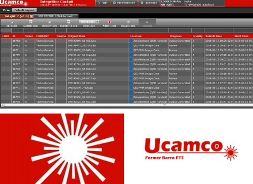
Based on example of the Argos 8008 tester (fig. 1) from Mania, the parameters, coarse and possibilities of optical testing will be discussed. This tester thanks to image scanning with a 5000 DPI resolution (dots per inch) enables the optical inspection of the plate surface with a precision of 2 mils. The scanning time of a single production format, depending on the selected level of inspection precision, lasts tens of seconds.

Fig. 1. Argos 8008 optical tester.
AOI testing procedure
The first stage of AOI testing is to prepare the test program. This includes marking on the image of the production format the areas excluded from the test and the placement of three reference points for each of the layers intended for basing the tester mechanics. Due to the small number of operations, this stage takes a maximum of 2-3 minutes or even less for simpler projects and so this is the quickest of the testing techniques discussed so far.
Optical testing proceeds according to the following scheme: loading the production format, basing the tester, scanning the top layer of the mosaics, detection of irregularities and their presentation on the attached monitor.
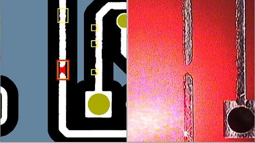
During damage classification, in order to reduce the number of detected deviations of the actual circuit image from the virtual model, tolerance areas are taken into account which allow for small displacements of the components of the scanned mosaic image in relation to the model. After checking one side of the laminate page, it rotates and repeats these operations. A view of example defects involving open and short circuits is presented in fig. 2, where missing mosaic elements (open circuits) are marked in red and redundant ones (short circuits) in green.

(a)

Fig. 2. Example screen shots of the Argos tester during open (a) and short (b) circuit detection.
AOI optical testing is characterized by high efficiency exceeding the capabilities of electrical testers. The discussed tester model has a daily capacity of up to 200 m2 of tested circuit surface area. Another advantage of AOI test is the ability to locate quality defects in mosaics and irregularities in some stages of circuit production which can be detected with electrical testing. The main limitation of optical testing is its inability to verify invisible layers—e.g. internal layers in compressed multilayer circuits and to control the correct metallization of the grommets. For these reasons, reputable PCB manufacturers, including TS PCB, in order to conduct comprehensive tests on manufactured circuits, use AOI testing as an intermediate control stage of the production chain preceding the final electrical testing.