


Yes. Those PCBs require chemical gold plating.
The minimum raster (figure one – the distance X) of such systems offered by Techno-Service is:
- for the vias 0,2mm: 0,8mm
There are certain situations (very simple BGA, without the paths connecting pads and vias) it is possible to use a smaller raster: 0,65mm.
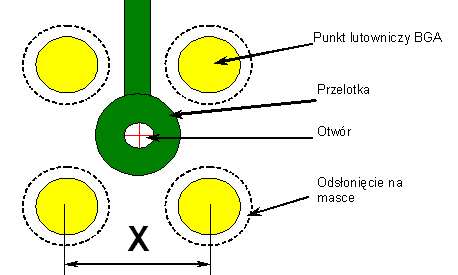 Figure 1. The exemplary BGA structure.
Yes. There are two types of plated PCB edges:
Standard edges plating
Metalization covers the edge on the straight section – there are no holes or half-slots on the edge. We advice gold plating in this case. It eliminates the risk of ckracking under the high temperature influence (e.g. during the assembling process).
Plating of the edges with half-slots or half-openings
On the PCB edge there are half-slots or half-openings (figure 1).
Figure 1. The example of plated half-openings on the PCb edge
In this case gold plating is necessary, as half-openings and half-slots are more exposed to thermal shocks.
It is worth to remember that the PCB edges which are supposed to be plated have to be milled as well – there is no possibility to use the scoring process in this case.
Yes – performing the electrical test is a guarantee to make 100% good boards. Orders in which it is required to perform the electrical test we are testing completely (all circuits). We use for this an independent testing device - nail tester (adapter), finger testers and tester of so called preliminary test (Acceler8).
Besides the electrical test we also perform the optical test for all produced circuits, including internal layers in case of producing multilayers circuits.
Such slots cannot be produced. The whole slot can be covered with soldermask or completely uncovered (the same refers to vias). In general we produce slots which are always uncovered (gold or tin plated). Slots which are supposed to be covered with soldermask have to be clearly marked in the project. The same rule applies to metallized edges of the PCB.
► Definition:
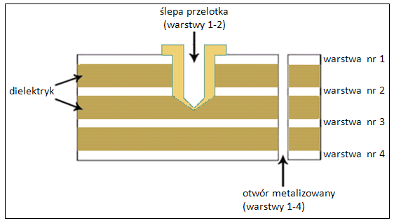
Blind vias are holes drilled only to a certain depth of the printed circuit.
This way they allow to connect a given external layer with a chosen internal layer/layers without necessity to drill through the entire thickness of the circuit. On the below illustration, the example of the blind via is shown made from the TOP side connecting it with the first internal layer. This, however does not mean that making from the second side of the printed circuit is not possible - such situation is clearly permissible. So, they can be made from the TOP side, from the BOTTOM side and from both sides simultaneously.
► Requirements:
Application of blind vias in the PCB project requires adopting to technological requirements. The first problem is the covering – you cannot use in their case the HASL/HAL type dip tin-plating method mainly due to a lack of possibility of removing the tin excess from such a hole.
The second restriction is dependence of the depth of the blind via from it diameter which is defined individually by the PCB manufacturer. In TS TCB this looks like this:
- For drilled diameters (the drill bit diameter, D) from 0.25 mm to 1.00 mm, the depth is 0.75*D;
- For drilled diameters (the drilling bit diameter, D) above 1.00 mm the depth is equal D;
Shown drilled diameter is the final diameter of the hole (assumed in the project) reduced by 0.1 mm. So, in relation to the final diameters above classification looks like this:
- For the final diameters of the holes (D2) from 0.15 mm to 0.90 mm, the depth is: 0.75*(D2 + 0.1 mm)
- For the final diameters of the holes (D2) above 0.90 mm, the depth equals D2+0.1;
► Application:
Bling vias are the most often used in so called HDI (High Density Interconnect) circuits that contain elements of high density of the connectors e.g. µBGA. They allow for the signal lead out from the via located between the soldering lands (or directly from the soldering land, so called via in the pad) through the internal layers instead of realization of such a connection with the traces located between pads. They allow also to better utilize available space on the circuit surface without necessity to increase it dimension – the via is not passing through the entire thickness of the laminate thanks to which the usable area from one side of the circuit is increased.
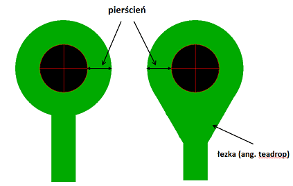
Minimum annular ring size depends on the number of layers and the layer type (inner/outer).
For the outer layers (no matter the type of the PCB), the minumum annular ring is always:
- 0.125 mm (5 mils) for FR4 laminates,
- 0,20 mm (8 mils) for aluminum laminates.
Standard minimum annular ring for the inner layers (multi-layer FR4 PCBs): 4 - 7 mils (depends on number of layers).
On the above drawing you can see how to measure the annular ring size – it is half of the difference of pad diameter and the diameter of the pad located in the mentioned pad. You can also see a teardrop pad on the picture.
.png)
Burried vias are holes which connect only the inner layers. This solution is used in multi-layer PCBs. Those holes do not go through the outer layers (see the drawing below).
By using burried vias the possibilities of PCB projectgive a lot of possibilities, e.g. the copper area in the inner layers is used a lot more effectively. It is also worth to use this technology in order to reduce the cost of the single PCB, as the burried vias do not increase the price as much as producing a PCB with more layers or increasing the circuit dimensions.
In order to create a project with burried vias, you need to take into account:
- maximum diameter of the burried via: 1,5 mm,
- gold plating of the outer-layers pads is necessary.
While creating a PCB project, please remember to maintain appropriate distance of conductive components from milling line, which will protect the circuits against electrical breakdown. Maintaining a proper space guarantees the insulation of conductive elements of the board.
Minimum values should be taken into consideration when determining the proper distance:
- minimum ground distance from PCB edge (milling line) is 0.20 mm (8 mils),
- minimum path distance from the PCB edge (milling line) is 0.25 mm (10 mils),
- minimum ground, path and pad distance from the PCB edge in inner layers is 0.20 mm (8 mils).
Minimum ground and path distance from scoring line depends on the laminate thickness – see the table below:
|
Laminate thickness (FR4)
|
0,55 mm |
0,8 mm |
1,0 mm |
1,2 mm |
1,55 mm |
2,0 mm |
2,4 mm |
|
Minimum scoring line distance to copper |
0,15 mm |
0,21 mm |
0,26 mm |
0,31 mm |
0,4 mm |
0,52 mm |
0,62 mm |
A few elements have impact on the final PCB thickness:
- the base laminate thickness tolerance,
- copper thickness,
- layers thickness (soldermask, metalization, cover, silkprint) – normally 0,17 mm.
The list of acceptable thickness of ready-made PCBs on FR4 laminate, 1 and 2-sided PCBs (total thicknesses) is shown in the table below.
| Base laminate thickness [mm] |
Base copper thickness [mm] |
Allowable thickness range of finished PCB [mm] | |
| min. | max. | ||
| 0,80 | 0,018 | 0,93 | 1,08 |
| 1,00 | Cu thickness included in the base laminate | 1,10 | 1,25 |
| 1,20 | 1,30 | 1,45 | |
| 1,55 | 1,65 | 1,80
|
|
| 2,00 | 2,07 | 2,27 | |
| 2,40 | 2,47 | 2,67 | |
| 3,20 | 3,24 | 3,50 | |
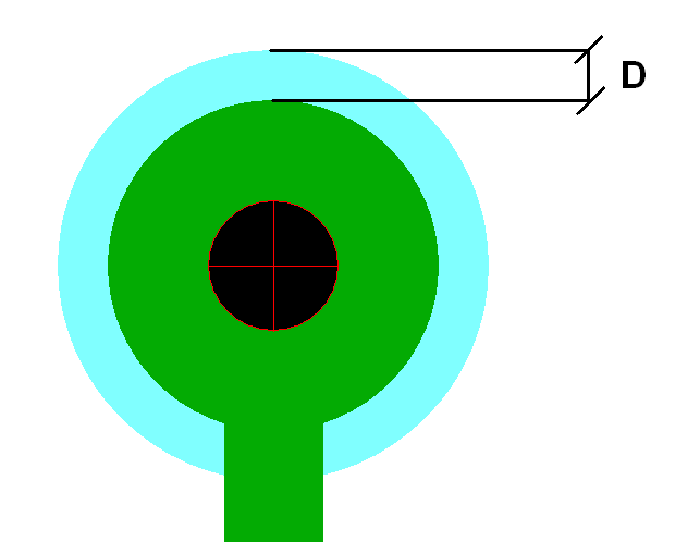 Pic. 1. Soldermask exposes the pad – D minimum exposure on each side.
Printed circuit board quality is strongly influenced by the design. At this stage the designer determines the production process and quality issues. Many small mistakes may be eliminated by introducing changes to the design. Hints applying to printed circuit board design are presented below.
Printed circuit board’s designer should not only take into consideration electrical quality but also production capacity of supplier. There are certain rules which should be followed in order to prepare a good project to be produced in our plant. Such rules can be found on our website; these are, inter alia:
- minimum distance between conductive parts,
- minimum path width,
- minimum holess diameters and rings sizes,
- minimum mask exposure,
- number of layers etc.
Every project has to be analyzed according to above rules. Fortunately, every deviation from these principles is easy to spot, since most modern systems for PCB design are equipped with checking and correction functions.
Due to the incorrect design, production problems may occur. It is worth to notice that such problems do not have to result from failing of complying with the rules mentioned above. These problems can also decrease PCB quality.
Copper surface and paths
One of the most common problem is incorrect copper distribution on outer layers. Efficiency of electrochemical processes of applying copper on PCB surface and into the holes is connected very strongly with the proper copper distribution on the PCB surface.
Printed circuit board surface with small number of elements (single insulated paths, holes) characterize with higher copper than other areas of the PCB with large number of elements or areas of copper.
Such solution results in the problem with maintaining holes diameter tolerance and correct soldermask applied on the edges of excessively thick paths in the areas with low number of elements. In order to improve copper distribution, additional copper surface is advised to be added in the area with small number of elements. Such non-functional copper area does not have any electrical function, but helps to obtain correct copper distribution in the electrochemical metallization process.

Figure 1. Not recommended solution, such situation should be avoided. Next: recommended solution – insulated paths and holes are protected with additional copper fill.
Another issue is the over-running minimum-width paths. Single insulated paths with the minimum allowable width cause digestive problems of printed circuit boards. Such paths are easy to be etched and exposed to mechanical damages and openings. It is recommended to reduce the length of paths with minimum width during the designing process. It means we run a 6-mil path in the heavily packed areas, but as soon as the density decreases, we increase the track width by 2-3 mills. An example is shown on Figure 2.

Figure 2. Figure 2. Not recommended, two bottom paths are exposed to etching and mechanical damage. Next: Recommended solution – paths with minimum width were expanded so both etching and mechanical damage are limited.
Teardrops next to pads
Quality issues of printed circuit boards are caused by the lack of ‘tear’ next to small pads (rings) very often. It happens that drilled hole is tangent to the edge of the pad. Such solution is allowed only if a hole is not tangent to the edge of the pad in the area of path and pad connection.
At this point the risk of gaping increases significantly. In order to protect against such problems, a special “tear” is added to the pad. It should overlap the path by not less than 5 mils. This rule is particularly important for small hole diameter (0,3 mm and lower) with minimum acceptable rings, where the probability of the defect of non-centric hole rises due to the insufficient rigidity of the drill.

Figure 3. Standard pad and the one with teardrop added.
Another reason for quality issues is free space between pads and paths (width of less than the acceptable minimum, e.g. 6 mils). After the exposure and development, the 6-mil (or less) photopolymer strip has limited adhesion. It often happens to detach and stick to the other area of the PCB. It results in shorts and opens depending on technology. This problem is presented on Figure 4. Figure 5 presents recommended solution.

Figure 4. Space between the bottom pad and path is too small.

Figure 5. Correct solution – correct distance between pad and path.
Distances
Another cause of errors are areas covered with soldermask of width < 5 mils. Such places also have reduced adhesion and tendency to flake (the same goes to photopolymer). It is noticeable especially on gold plated PCBs (damaging effects to the soldermask).
Such surface should be extended or removed from the project. Small residues of copper on the board also have a big impact in this case. PCB’s designer should pay particular attention not to leave unnecessary remnants of copper.
Copper remnants have very poor adhesion to the laminate and may cause short circuit when applying the mask. This problem is presented on figure 6. Also the large difference between the top and bottom surface of copper result in low quality of the PCB.
Such difference causes tension. This types of PCBs have a tendency to bend in heat treatment. It applies especially to the PCBs thinner than 1,5mm. In such cases it is advised to use additional copper fulfillment on the side with lower surface or copper grid on the side with higher copper surface.
Such solution relieves the tension and there are no PCBs’ deformations. Figure 7 presents copper grid instead of masses with the whole copper surface. While creating such grid, it is good to remember that the side of the empty square should be minimum 8 mils and the thickness of copper line no less than 10 mils. The last issue is creating the large surface without copper on the inner layers of PCBs.

Figure 6. Accidental part of copper.
<img alt="Using of the grid instead of mass with the full cooper surface." height="183" web="" uploads="" images="" 1638547e4f08bd3a979ea9c3ef390a82.jpg"="" style="display: block; margin-left: auto; margin-right: auto;" title="Rys. 7. " width="284">
Figure 7. Using of the grid instead of mass with the full cooper surface.

Figure 8. Not recommended solution – black area on the PCB is the low pressure area. Next to it, recommended solution – empty area has been filled with copper.
During the pressing process, such places create so called areas of low pressure. Such areas require large amount of resin to fill it utterly. If there is not enough resin, empty vesicles are formed (that resembles of delamination process). The solution is to add in non-functional copper surface (which is presented on figure 8). Compliance with this rule is particularly important for the projects with copper thickness ≥70μm.
Efficient use of laminate
PCB’s designers have also an impact on the final price of the circuit as far as the use of laminate is concerned. Solutions used by them may have great impact on the efficiency of the laminate use. Since PCBs are not produced as single pieces but in a production format (e.g. 460×610mm). PCBs producers advice clients to contact them to discuss the optimum panel size resulting in high efficiency of material usage.
It happens very often that adding one single PCB to the panel or removing it greatly reduces the wastage of laminate.
Issues presented above result from the mechanical and physiochemical feature of material and process used for PCBs production. The PCBs designed following the above rules will be a lot easier to produce, which means that we can produce it faster, better, cheaper and also avoiding the risks connected with the quality problems.
While determining proper holes’ diameter, one must take into account all limitations – that is to say, minimum hole diameter for selected laminate thickness and tolerance parameters. Minimum hole diameters are specified in the table below:
|
Laminate thickness [mm] |
Minimum allowable PTH diameter after metalization (mm) |
|
1,55 |
0,15 |
|
2,00 |
0,20 |
|
2,40 |
0,20 |
|
2,50 |
0,25 |
|
3,00 |
0,30 |
Plated hole diameter, due to the galvanic copper layer, is smaller by about 0,1 mm relative to the diamater of the drill. That is the reason why when determining the minimum non-plated holes’ diameter, you need to add 0,1mm to the diameters from the table above (e.g. for the 1,55mm laminate the minimum non-plated hole diamater equals 0,25 mm).
You also need to remember that the standard tolerance of the plated and non-plated holes’ diameter is + 0,1 mm / – 0,05 mm. If your project has some specific parameters as to the holes’ diameter tolerance, please remember to emphasize it in your order. It is worth to notice that there is no possibility to produce PCBs with the holes’ diamater tolerance of +/- 0,00 mm.
The base thickness of laminate for multilayer PCB normally includes the total thickness of the core(s) with base copper foils: external and internal.
The maximum allowable tolerance for the final laminate thickness is ±10%.
- precise PCB final thickness with tolerance results from:
- prepregs thickness – average ±0.007 mm;
- core thickness described in tab. 1;
- process – typically ±0.03 mm.
| Core thickness [mm] | Tolerance [mm] |
| 0.10 | ±0.01 |
| 0.20 | ±0.02 |
| 0.36 | ±0.03 |
| 0.50 | ±0.04 |
| 0.71 | ±0.04 |
| 1.00 | ±0.06 |
Tab. 1. Core thickness tolerance
For multilayer PCB with ≥70 μm conductive layers, the final thickness depends on the final thickness of copper due to the necessity of applying a thicker layer of mask as well (presented in tab. 2.).
| Copper final thickness [μm] |
Coating thickness [mm] |
| 35 | 0.17 |
| 70 | 0.22 |
| 105 | 0.25 |
Tab. 2. Thickness of applied coatings
A method for defining the final PCB thickness based on the standard structure of a 4-layer PCB (thickness: 1.55 mm) --- ► link and its tolerance is described below.
A standard 4-layer PCB structure includes:
- 4 prepregs, type 7628 – thickness P=0.72, ±0.028 mm each,
- core 0.71mm (plus two copper layers 2 x 35 μm) – thickness R=0.78 ±0.04 mm.
- base copper on outer layers: 2 x 18 μm.
The final thickness and its tolerance will be P+R+0.03 mm (process tolerance) + 0.17 mm (application of coating) = 1.706 ±0.1 mm.
This is the basic method for calculating multilayer PCB final thickness and its tolerance. However, this method is considerably theoretical and does not always prove to be effective. Should more accurate values be necessary, MultiCal software can be used to provide precise estimation of laminate thickness after pressing while considering additional parameters.
We offer the following PCB types:
- one-sided on the laminates: FR4 (non-plated holes), aluminium (non-plated holes), Rogers – laminate dedicated for high frequency (plated and non-plated holes);
- double-sided on the laminates: FR4 (non-plated and plated holes), aluminium (non-plated holes), Rogers – laminate dedicated for high frequency (non-plated or plated holes, depending on the laminate type);
- multi-layer – up to 8 layers on the FR4 laminate (non-plated or plated holes).
V-cut scoring involves cutting the laminate to a certain depth (on one side or on both sides of the plate) to allow it to be later broken off from the panel. It is usually described with two parameters:
- Incision angle (standard 30°),
- Non-v-cut scoring thickness.
Thickness of the non-v-cut scoring item and the type of Non-v-cut scoring (single-or double-sided) is dependent on the thickness of the used base laminate. The dependencies are shown in the following table.
|
X [mm] |
A [mm] |
Comments |
|
≥ 0.5; < 0.8 |
0.15 |
Single-sided V-cut scoring |
|
≥ 0.8; < 2.4 |
0.3 |
Double-sided V-cut scoring |
|
≥ 2.4 |
20% * X |
Double-sided V-cut scoring |
Minimum soldermask amount on the path edge is 7 μm, independently from the final copper thickness
The soldermask thickness on the ground areas are:
- 50 μm for the final copper of 35 μm,
- 85 μm for the final copper of 70 μm,
- 120 μm for the final copper of 105 μm.
Any other soldermask thickness should be consulted individually before placing an order.
Outer edges of PCB are milled by standard tools with a diameter of 2.0 mm. The use of such a diameter allows to shorten the time of milling and increase its accuracy. In order to mill edges at long distances, do not use smaller cutters because of the difficulty in obtaining high milling accuracy (tool bending) and longer milling operations (possible increase in a price).
In addition to the cutter of 2.0 mm, standard diameter tools are also used: 0.8 mm; 1.0 mm; 1.2 mm; 1.5 mm; 2.4 mm. In addition, there are also all the diameters ranging from 0.6 mm to 2 mm (0.1 mm).
In the multilayer PCB order form, the base laminate thickness is defined. It consists of: core thickness (with 35 mm copper) and the outer copper foil (18 mm). The maximal final laminate thickness tolerance is ±10%. For the standard 1.55 mm base laminate the thickness tolerance is 1.55 ±0.155 mm, which means the final thickness of between 1.395 mm to 1.705 mm. The existence of thickness tolerance (range) is caused by the tolerances of:
- prepregs – ±0.007 mm,
- core (see the table 1),
- production processes – typically ±0.03 mm.
Tab. 1. Core thickness tolerances.
|
Core thickness [mm] |
Tolerance [mm] |
|
0.10 |
±0.01 |
|
0.20 |
±0.02 |
|
0.36 |
±0.03 |
|
0.50 |
±0.04 |
|
0.71 |
±0.04 |
|
1.00 |
±0.06 |
In case of multilayer PCBs with thicker Cu (conductive) layers – 70 mm or more – the base laminate thickness increases. For the PCB with a core Cu of 70 mm the thickness will be 1.62 mm (1.55 mm + 0.07 mm), because the standard thickness must be increased twice as the result of additional 35 mm Cu thickness of a core. The final PCB thickness is the total thickness of the base laminate and coatings applied in the production process: galvanic copper and soldermasks. Thickness of coatings depends on the final copper thickness (hight) as it is shown tab. 2. The higher the mosaic layers are, the thicker coatings have to be placed, because the soldermask has to be thicker in order to be permanent, especially on the mosaic edges. Next to tab. 2 the calculation example of thickness and its tolerance for typical 4 layer ML PCB (stuck-up) is shown.
Tab. 2. Applied coatings thickness.
|
Finall copper |
Coatings |
|
35 |
0.17 |
|
70 |
0.22 |
|
105 |
0.25 |
The standard 4-layer stack-up consists of:
– 4 x prepregs 7628 – thickness P=0.72 ±0.028 mm,
– core 0.71 mm / 35 mm – grubość C=0.78 ±0.04 mm.
Therefore the final thickness and its tolerance is P + C+ 0.03 mm (process tolerance) + 0.17 mm (applied coatings) = 1.706 ±0.1 mm.
In order to get the standard thickness PCB for thicker copper layers, please place such information in the “Customer’s remarks concerning PCB fabrication” field in the order form. This type of information should also be added in case of unusual laminate thicknesses and tolerances.
PCB plating method is always specified by the client, although it is not arbitrary, since the plating methods have some limitations. Tin plating is more cost-effective, although the quality compared to gold plating is lower. It can easily be chosen for less complicated printed boards. For more complex designs, gold plating is recommended. In many cases, there is no choice. For technical reasons some of the printed boards cannot be tin plated.
Gold plating has to be used for circuits with:
- BGA,
- distance width 100 µm (4 mils) or less - for two exposed copper elements,
- pads ≤ 200 µm (8 mils) for one-sided SMD,
- pads ≤ 300 µm (12 mils) for double sided SMD,
- blind vias,
- buried vias,
- base laminate thickness of less than 0.36 mm,
- half-slots and half-apertures on the edges.
Gold plating should be used not only if this is necessary for technical reasons but also if high resistance to external factors, smooth pad surface and perfect soldering capabilities are required. By selecting this plating method, we make sure that the nickel layer protects copper plating against dissolving during assembly, which must be adapted for gold.
Gold plating is also required when:
- the project includes edge connector (flatness),
- the edges are plated.
There are four types of vias in our offer:
1. Vias: vias which are covered with soldermask. This type of vias are not plugged, the paint goes through the vias with curtain method covering edges and inside walls of these holes.
2. Plugged and covered via – standard: vias are plugged with special photochemically cured paint before PCB surface is covered with soldermask. Vias are 100% plugged and covered with soldermask. They are filled with paint in about 40%. Thanks to the mentioned paint, solder does not reach the other side of the circuit – however the vias surface is not flat. This method is suitable for plugging the vias in leadfree HASL technology, as well as gold plating, with final copper thickness of 35µm. It can also be used for plugging holes with the maximum diameter of 0,6mm.
3. Plugged and covered via – flat: if you want a via to be more flat (and therefore increase the degree of filling it with the paint), you can choose this method of plugging; filling ratio is > 80%. Applying this method requires the use of gold plating technology – such circuits cannot be produced with leadfree HASL cover. This method can also be used for vias plugging on the circuits with final copper thickness of ≥ 70μm. This type, like the previous one, can be used for plugging holes with the maximum diameter of 0,6mm.
This method can also be applied for plugging vias in the pads, however the paint used to plug the vias is not covered with copper, and there is a 3 mils paint areola around the hole. When ordering this type of plugged vias, please add the note “FLAT VIAS” to your order.
4. Plugged via – vias are plugged after the covering process (gold plating, HASL), using the special paint (silkscreen technology) and thermally cured. Vias are plugged, however with a bit of a bulge. The paint is visibly standing out beyond the copper surface. This type of vias is suitable for plugging holes with the maximum diameter of 1mm.
While preparing the project, restrictions regarding the diameter of the plugged via have to be taken into account. If the via diameter equals 0,5mm, any type of via can be selected. If the via diameter is e.g. 0,8mm, only the plugged via type is an option.

