
Structure, characteristics and design of multilayer printed circuit boards
Łukasz Romik Author
Modern electronic devices are expected to deliver high functionality, small form factors and high reliability. These features are achieved with large numbers of miniature and composite integrated circuits which are interconnected by complex networks. Mapping those IC’s on a typical double-sided printed circuit board is not possible due to e.g. the required and limited dimensions of the PCB alone; hence multilayer PCBs are necessary, and sometimes in HDI (High Density Interconnect) versions that typically include 4, 6, 8 or more conductors layers, the so-called mosaics. This paper presents the structure, manufacturing and proper design methods of multilayer PCBs. Following the latter will help to avoid problems at the stack design stage and in the subsequent manufacturing process of the PCB.
Structure of a multilayer PCB

Fig. 1. Layer arrangement in a 4-layer PCB, (a) Type 3 and (b) Type 4.
Unlike double-sided PCBs, the structure of multilayer laminates is far more complex. It is stacked-up or built-up and has an organised layered structure, which is usually arranged symmetrically around its centre. The cross-section of the laminates discussed herein feature three components: copper foils, cores and prepregs, where the latter are usually made of type FR4 laminate. The arrangement of the components is explicitly established in the standard IPC 222 which strictly defines two types of multilayer stack arrangement: Type 1 and Type 2. Both layer arrangement types are shown in Fig. 1 with a 4-layer PCB.
Type 3 stacks are used sporadically, mainly in simple designs. This arrangement type does not permit building buried vias which connect the inner conductor layers, whereas building blind vias is problematic. The only advantage of Type 3 stacks is that they are slightly stiffer than Type 4 at the same laminate thickness, especially in designs that involve highly differentiated copper surface areas of the conductor layers.

Fig. 2. Cross-sections of 4, 6 and 8-layer PCBs (a, b, and c, respectively).
Type 4 is the most popular multilayer laminate arrangement of layers and predestined for the manufacturing of complex designs. This type has been applied by many PCB manufacturers, including TS PCB. Type 4 allows building buried vias on cores and relatively simplifies the drilling of blind vias. Moreover, Type 4 permits joining prepregs of various thickness together and thus assures a high flexibility of thickness forming for the prepreg layers and the overall laminate layer. Hence the following part of this paper will discuss Type 4 multilayer PCBs.
Examples of 4, 6 and 8-layer PCB stacks are shown in Fig. 2. The figures show that the stack interior features cores that comprise a dielectric coated with copper foil on both side and have a double-sided laminate structure. These form the inner conductor layers in multilayer PCBs. The outermost external stack layers comprise copper foils with the top and bottom layer mosaics mapped on them. The cores are separated from the Cu foil layers with the prepregs which are intended to bind the stack firmly and permanently with the required spacing of the components.
Materials for multilayer PCB construction
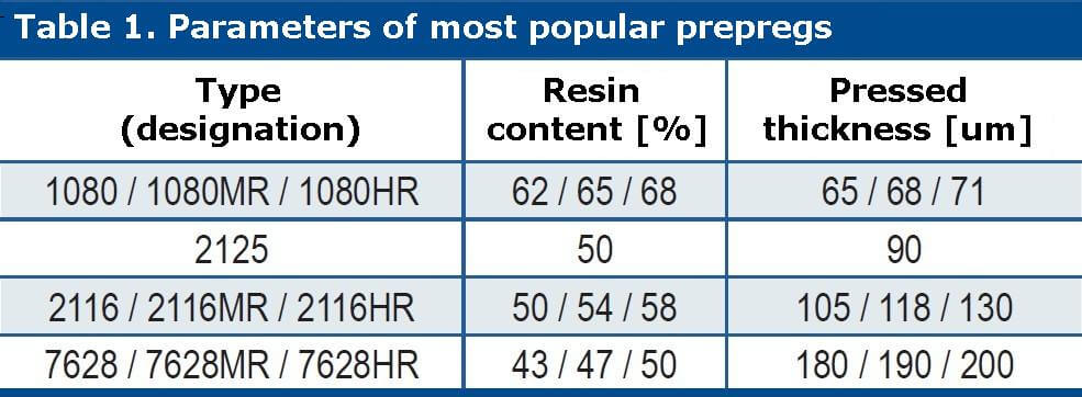
Table 1. Parameters of most popular prepregs
All parameters of multilayer PCB components are standardised, especially the thickness values. The following shows the catalogue master data of the most popular prepregs, cores and copper foils.
Prepregs are manufactured in the form of single glass fibres that are saturated with partially polymerised epoxy resin. A pressing process is applied during which high pressure and high temperature melt the fibres, which binds the individual stack layers together. There are many commercially available prepreg types which vary in thickness and resin content.
However, most PCB manufacturers carry 3 or 4 types in their ranges (Table 1) that guarantee good quality parameters of PCBs and optimum flexibility in stacking up. This has been mainly caused by cost effectiveness. Prepregs have a relatively short shelf life, so stocking up on many varieties of the material would expose PCB manufacturers to high losses due to the necessary refreshes of many prepreg types, especially those less popular in use.
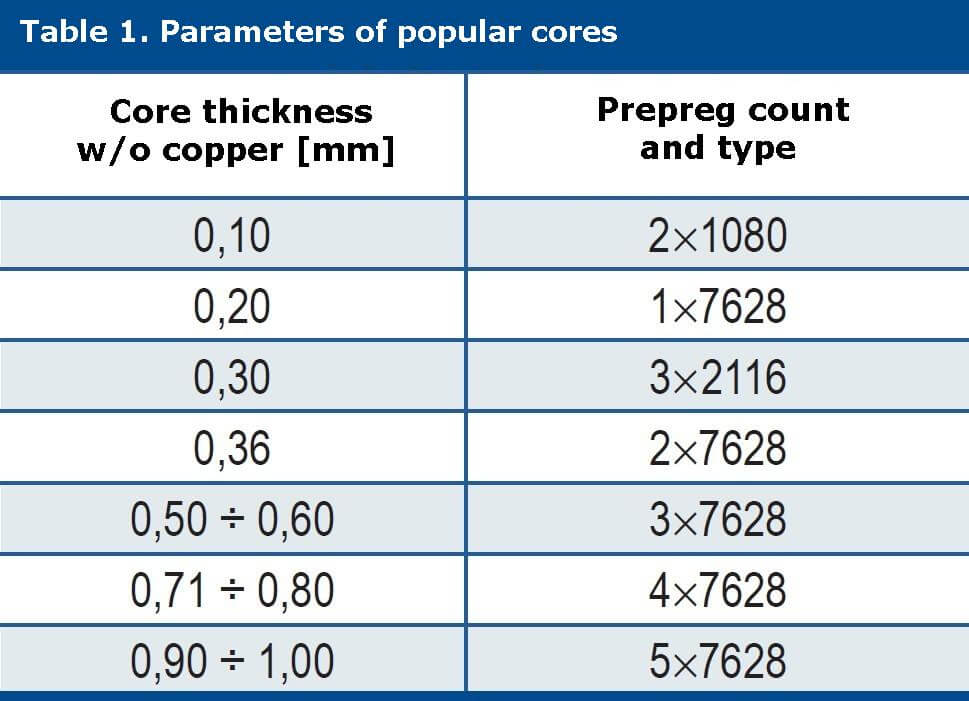
Table 2. Parameters of popular cores
As pointed out above, cores are double-sided laminates with copper coating, available with the following standard thickness values: 18, 35 (standard), 70 and 105 µm. Not unlike with prepregs, the core thickness values include the Cu foil thickness are standardised and form a type series. The available typical core thickness values and the prepregs used to build the cores are shown in Table 2.
PCB manufacturers carry ten or so of the most popular cores on average, and which are also available with various Cu foil thickness values and in versions with improved Tg (150 and 180°C). The Cu foil thickness range is similar to that of the cores: 18, 35, 70 and 105 µm. The finished copper thickness values downstream of the metal plating process can be as follows: 35 (standard), 70, 105 and 140 µm.
Principles of PCB design
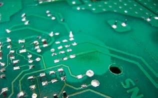
Fig. 3. Example of delamination.
The process of multilayer stack design involves selecting component parameters that will guarantee the designed electrical performance (current, impedance and breakdown resistance values) and mechanical characteristics (thickness, stiffness and workability) of the laminate. This means choosing the parameters of:
- The cores to obtain the designed number of layers, the spacing of inner layers within each core and the thickness of the inner conductor layers;
- The prepregs that give the correct spacing of the cores, and between the cores and outer mosaic layers at the sufficient resin fill level;
- The Cu foils, inclusive of the DRC parameters of the PCB outer mosaics.
The structure of a multilayer stack shall include the processing capacities and the material range at the disposal of the relevant PCB manufacturer at the design stage. Highly non-standard or highly sophisticated cores and prepregs and/or their arrangement may, in extreme cases, render production of the designed PCB infeasible.
In this case PCB manufacturers usually propose alternative build-ups with the parameters as approximate to the original construction, but built with materials at their disposal. Insisting on building a core from atypical materials, which must be ordered externally, will definitely increase the lead time and costs of the project – assuming, of course, that there are no other processing hurdles that prevent manufacturability altogether.
It is recommended to use cores that are symmetrical relative to the cross-section centre to achieve approximate surface stresses on both sides of the laminate. This also applies to the copper distribution across the mosaics, and especially on the inner layers. Symmetrical build-up is sometimes impossible. For example, this can be caused by very specific transmission line impedance values, resulting in warping of finished PCBs at the assembly stage (soldering).
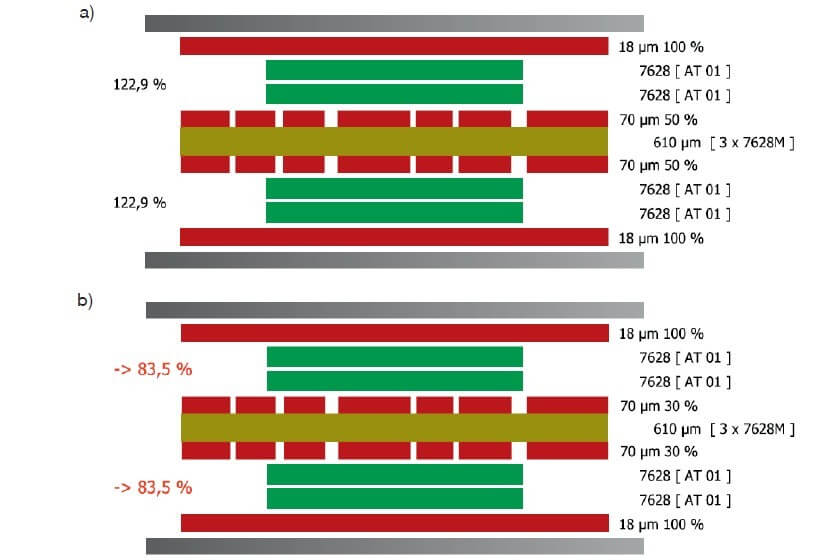
Fig. 4. Overview of a build-up with a (a) correct and (b) insufficient resin fill level in Multical.
The stack build-up must follow the principle of applying a minimum of two prepregs to separate adjacent conductor layers. Using one prepreg only may result in leakage of currents and development delamination foci, since at the pressing stage of the PCB the glass fibres may become damaged, especially along the edges of mosaic features.
The number and type of prepregs is critical to the resin fill level between the conductive layers, and also depends on the conductor layer thickness and copper fill level. Insufficient resin fill levels cause an effect called ‘resin hunger’, where empty voids appear between the laminate layers with a potential to delaminate and separate the layers of the build-up (Fig. 3). If galvanic products are trapped inside the voids, they may evolve into foci of corrosion or current leakage.
The best method to check the required resin quantity is to use special software for the design and checks of multilayer cores; leading laminate manufacturers offer freeware versions on their websites. The most popular programs are Multical (from Isola) and Multilayer Architekt (from Technolam).
The figures show a comparison of two cores developed in Multical: one with a correct resin fill level (Fig. 4a) and the other with an insufficient resin fill level (Fig. 4b). The resin insufficiency problem has several solutions: (i) increase the copper surface area on the inner layers, (ii) use prepregs with a higher resin content (mark MR or HR), or (iii) add a prepreg, which, unfortunately, will increase the thickness of the dielectric and the whole laminate.
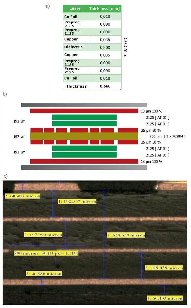
Fig. 5. Comparison between the layer thickness values (a) as calculated, (b) as determined in Multical and (c) as measured in an actual 4-layer PCB.
Another value of using the said software is the capacity to determine the layer spacing and the finished laminate thickness after pressing more precisely than possible with traditional mathematical methods. Fig. 5 shows a comparison between the layer spacing in an example of a 4-layer stack as defined by calculation, as determined in Multical and as measured with microscopic imaging of the microsection.
In this case the PCB designer assumed that the layer spacing must be 180 µm. Hence two 2125 prepregs were used as guided in Table 1. However, when the PCB was designed in Multical – and the software accounts for the copper surface areas across the inner layers and the resin content in the prepregs – it became clear that the total thickness of both 2125 prepregs is ca. 10 µm larger.
The microsection of the actual PCB confirmed that the dielectric is about 190 µm thick, which is very approximate to the value output from Multical. Reaching full compliance of the prepreg layer thickness and cores with the Multical outputs is highly improbable due to the thickness tolerance of materials.
Some designs of electronic circuits, e.g. for high-voltage applications, require cores over 1 mm thick. These cores are usually not on PCB manufacturer stock, because are not popular. It is still possible to produce them indirectly: by pressing two thinner cores that are separated with prepregs. In this case the core stack-up is Type 3, but it also features a digested layer of copper inside. Fig. 6 shows an example PCB stack with a 1.6 mm thick core.
Buried and blind vias are applied to increase the packaging density of multilayer PCB components. As discussed before, buried vias allow joining the mosaics within single cores and free up the surface of the outer layers, e.g. for assembly of other components. Note that there maximum buried via diameter is limited by the risk of delamination focus development. TS PCB recommends buried via diameter values of 1.5 mm maximum.
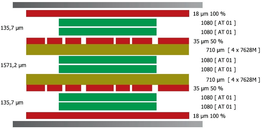
Fig. 6. Example of a stack with a 1.6 mm core.
Blind vias allow joining one of the outer conductor layers with one or more inner layers. Unlike with regular vias, this frees up the space on the opposite outer layer which can be then used to e.g. trace out the connection networks.
A certain limitation of blind vias is the dependence of the blind via diameter on the permissible drilling depth, and the resulting potential number of layers to be connected. Blind vias can be reduced in size with the minimum spacing of joined layers. It is recommended (unless there are no contraindications) to use blind vias on thin laminates that are less than 1 mm in thickness.
If a higher thickness is required, it is better to design the PCB with the blind rivets joining only the outer layers with their nearest inner layers, separate the layers with two 1080 prepregs, and produce the expected finished thickness of the laminate by applying thicker cores.
Summary
The paper discusses the build-up of multilayer stacks, the parameters of component materials, and principles of good PCB design. Tools are discussed which aid in the stack design process and guarantee proper resin fill level for the required finished thickness of the prepreg layers and the laminate as a whole. Compliance with these principles will help avoiding many problems related to the manufacturing and assembly of the discussed PCB types and the associated extra costs.
Show more from category Quality
-
Quality

Manufacture of printed circuits in harmony with the natural environment - environmental solutions
-
Quality

Manufacture of printed circuits in harmony with the natural environment - recycling
-
Quality

Manufacture of printed circuits in harmony with the natural environment - legal requirements
-
Quality
Manufacture of printed circuits in harmony with the natural environment - waste classification, storage and disposal
-
Quality

Testing printed circuits: AOI optical testing
-
Quality

Testing printed circuits: Blade testers
-
Quality

Testing printed circuits: Finger testing – testing time optimization
-
Quality

Testing printed circuits: Electrical testing – testers with moving probes
-
Quality

Testing printed circuits: Classification of the circuits testing methods and introduction to electrical testing
-
Quality

Base material of printed circuit boards: a few words about laminates
-
Quality

Certificate ISO 9001:2015 and 14001:2015
-
Quality

IPC circuit classes