Printed circuits. Typical errors in production documentation. Part 1
25.11.2015

The contents and quality of electronic production documentation for printed circuit boards (PCBs) is decisive to the time and cost of finished PCB production. Vague and imprecise information often leads to great problems in proper interpretation of actual customer requirements and, in extreme cases, may lead to manufacturing of non-conforming PCBs. This article discusses the typical errors found in the production documentations that are best avoided. The presented resulting defects are appended with recommendations and tips that warrant efficient production of PCBs that fully meet customer's demands.
This work is divided into two parts, due to the sheer volume of issues it discusses. The first part presents the contents of production documentation, the applied file formats, and the typical errors found in individual design layers. Part two, which will be featured in the next issue, will discuss typical errors of automatic assembly panel structures and build-ups of multilayer PCBs, and a selection of errors in design processing specifications.
Production documentation contents. File formats in use
A complete PCB production documentation is a technological (processing) specification and the PCB design in the form of essential files which hold the individual design layers. A major error is the lack of one of the documentation components and missing sets which the existing design files refer to. When incomplete, the production documentation most often extends the project lead time due to the clarifications necessary to amend it. Not only a production documentation should be complete, but the delivered design files must be available in formats that are generally accepted in the PCB industry.
The popular file formats for PCB designs accepted by the majority of leading PCB manufacturers include: Gerber (versions RS274X or RS274D), Excellon, and ODB++. Many popular CAD programs have the option to export data to those formats. Some manufacturers may process other and less popular file formats that are native to the software suites they use (e.g. CAM350, Lavenir, Ucamco, or Graphicode). A design sent to a manufacturer in the internal format of the CAD software used, i.e. usually as a single file, is most often unreadable and cannot be manufactured.
Pc technical specification should be easy to read in typical word processors, popular image file viewers or PDF readers. It is tolerated (and in use) to save those parameters and other auxiliary information in graphic formats on additional design layers. A specification can be saved to one or more files, which may improve readability, provided that the information is grouped in a sensible way. This solution is commonplace in more advanced designs prepared as panels for automatic assembly. The individual data sets usually present (i) design processing parameters, (ii) dimensioned drawings of the panel and its details, (iii) specifics of routing, and the laminate cross-section which shows the desired PCB stack-up. The number of files notwithstanding, it is key to present the set contents and nomenclature that are clear and explicitly understood. Long names, especially that contain series of digits, is an unnecessary risk of omitting a file or studying a wrong file when the documentation is reviewed.
A good production documentation contains the minimum number of files required to make it complete, and an easy and explicit interpretation of the information that is saved in a language accepted by the PCB manufacturer. Usually the PCB manufacturers accept documents in English or German, aside from their native languages. While the production documentation for simple designs in other languages can sometimes be accepted, more advanced designs might be returned with requests for translation into a more commonplace language.
Redundant files that are not useful for PCB production make reviewing the production documentation difficult. This mainly applies to large groups of files for automatic assembly (i.e. BOM and Pick & Place), catalogue memos on components, too extensive commissioning and functional testing manuals for assembled packs, or notices of changes in individual design revisions. It is unacceptable to provide various design revisions or several processing specifications in one production documentation package, especially if the revisions or specifications are contradictory. Appending filled out processing sheets available on PCB manufacturers' websites is a good idea.
The easiest way to order PCB production is to provide the PCB manufacturer with the production documentation by e-mail, along with the required number of products and delivery date. However, it is recommended as the best solution to submit orders on-line via web forms of the PCB manufacturers. The parameters input in the web form automatically generate the processing sheet in the PCB manufacturer's system, whereas the integrated control mechanisms reduce the risk of grave processing errors already at the ordering stage. Another advantage of e-ordering is the automatic pre-verification of the enclosed design documentation for completeness. This feature is offered by top PCB manufacturers, including TS PCB and run at the order submission stage.
A design documentation that has all required files enclosed can still have errors or inconsistencies in its contents. The following part discusses the most common defects of this type in individual design layers.
Mosaic layer defects
The most common design documentation errors that appear on the mosaics is the failure to comply with the minimum DRC (Design Rule Check) parameters, placing parts of the mosaics outside the PCB outline, or embedding auxiliary layers that improved the automatic assembly processes.
The DRC parameters the characteristics of which at various Cu foil thickness values is available in the PCB manufacturer processing specification define the minimum permitted spacing and width values of mosaic components at the preset copper layer thickness. Note that DRC values increase directly with the Cu foil thickness, which means that it is impossible to deliver a design with 5 mils
(0.127 mm) wide paths when the finished copper thickness is 105 μm. A design with the DRC values less than the permissible minimum precludes manufacturability. Some manufacturers, like TS PCB, offer technical assistance and suggest what needs to be changes in the design to enable or optimise production.
(0.127 mm) wide paths when the finished copper thickness is 105 μm. A design with the DRC values less than the permissible minimum precludes manufacturability. Some manufacturers, like TS PCB, offer technical assistance and suggest what needs to be changes in the design to enable or optimise production.
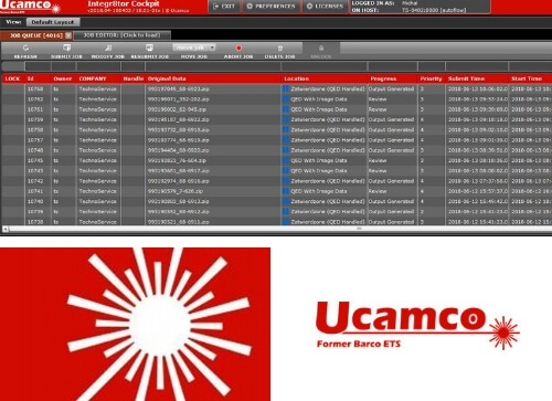
Fig. 1. Details of the mosaic and holes (framed in red) outside the PCB outline (pink line).
Mosaic parts extending beyond the PCB outline (see Fig. 1) may mean to a PCB manufacturer that the provided design documentation is incomplete or still a draft and requires clarification. It is then worth it to build a habit of removing obsolete parts of designs that extend beyond the PCB outline before generating the files for production.
Many PCB CAD programs can create extensive production documentation that is also fit for automatic component assembly. The programs generate additional layers with outlines of assembled electronic components and other special markers that can be easily embedded in other layers when Gerber files are generated. Customers sometimes accidentally use those options and while the consequences can be dire for the overall design, they are usually easily caught by PCB manufacturers. While embedding additional symbols on resist layers or text is relatively harmless, they usually cause short circuits when present on mosaics (see Fig. 2). A design affected by this has an incorrect electrical junction network, even if it follows the enclosed documentation. This requires particular attention to be given to the options selected in the CAM processor that is responsible for generating the design production files. It is also important to visually check the generated Gerber files in freeware viewers, such as Gerbv for any and all irregularities.
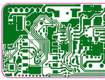
Fig. 2. Example of the embedding of automatic assembly auxiliary layers on a mosaic that result in numerous short circuits.
Defects of text and resist layers
Similarly to mosaics, the parts that stretch outside the PCB area and onto the soldering resists and text must also be removed. The texts shall be made on resist layers with apertures the sizes of which match at least the minima recommended by the PCB manufacturer. This is especially critical since underneath the text is a copper layer that will be HAL tin plated. There is a high risk of incorrect tin deposition of the text. This does not reduce the electrical performance of a PCB, but the aesthetic value is affected (see Image 1).
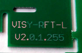
Image 1. Partially tinned text caused by an insufficient aperture size of the soldering resist.
The text layers shall have lines of at least 4 mils (0.102 mm). Thinner lines are permitted only when they overlap to form a larger character or symbol, e.g. a logo. Proper text production is impossible with smaller apertures, because even if enlarged to the required minimum, text symbols become illegible. Text symbols should not be placed on unmasked pads or vias since these will be trimmed against the soldering resist layer. Failure to follow this leads to intense 'slicing' of the text layer with loss of legibility and aesthetic value (see Image 2).
Image 2. Illegible text after trimming against the soldering resist.
Defects of machined layers
Depending on customer's requirements (e.g. use of plated edges, tapered holes, etc.), the individual PCB machining operations are carried out in several production stages. This is why the operations must have sufficient documentation. The basic machining layers is the outline that defines the form and size of the PCB.
Outline
The design must feature an explicit outline of the PCB. It is a closed polygon or curve. Missing outlines, multiple outlines or incomplete outlines disqualify designs from production. The outline must be placed on a separate layer. Embedding the outline on several or all layers of the design is a bad idea; this may cause shorting across the mosaics and make the proper PCB shape definition difficult. The design documentation for PCBs in panels should contain the outlines of individual PCBs and the panel itself. Several outlines offset against each other, improperly closed polygon corners or partial lines and other markers outside the actual PCB outline or within the PCB makes it very hard for CAM engineers to define the proper shape of the PCB. These are the most common causes for design clarification.
Milling and scoring layers
Other objects and forms on the outline layer may be interpreted as subject to additional machining. Hence this type information (e.g. specification of routing) is best placed on separate auxiliary layers called 'mechanical layers', and the use of the layers must be explicit in the processing specification.
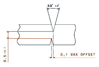
Fig. 3. Example of a good designation of scoring depth and permissible score line offset.
It is a good practice, especially if the machining (by milling and scoring) of panels and PCBs is complex. Designers may define the depth of scoring (see Fig. 3). If that information is missing, the PCB manufacturer will apply the default processing depth for the designed laminate thickness. The designs with feature z-routing should have the machined areas well marked and dimensioned, or at least there should be a clear text description of which PCB side must be z-routed, and to what depth (see Fig. 4).
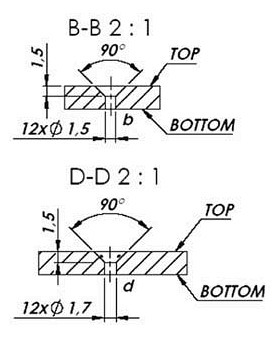
Fig. 4. Example of a proper marking of z-routed taper holes.
Chamfer layer
The rims of edge connections in PCBs are usually additionally processed by chamfering to facilitate the downstream assembly of the pack in the finished device sockets. Chamfering should be clearly defined in the processing documentation or directly on an auxiliary mechanical layer by indication of the chamfered area with the chamfering angle (which is typically 45° or 30°), as shown in Fig. 5. If the chamfering angle is not specified, the PCB manufacturer will use a default value, it is usually 45°.
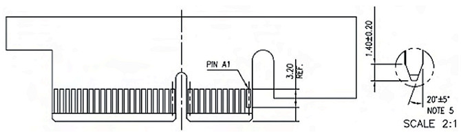
Fig. 5. Example of a properly marked joint mill.
Drilling
The typical defects in drilling programs include: missing tooling diameter values, use of various units in definitions of tool diameters and coordinates, use of the colon as a decimal character, and notation of coordinates in low resolution formats.
The drill tool diameter values that PCB manufacturers understand as finished values shall be specified in the drilling program header, although they can be also described in a separate text file. Use of inconsistent units for tooling sizes and coordinates, as well as of colon as the decimal character results in difficult data uploading to CAM software. In rare circumstances the problems may result in production of incorrect bores.
A rather rare error is to write the drilling program with insufficient accuracy of coordinates, caused by too few decimal places specified for unit values. A negative effect of this is non-centricity of the holes relative to their mosaic pads (see Fig. 6). The minimum number of decimal points required to keep the coordinates precise enough is three for millimetres and four for inches.
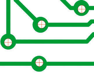
Fig. 6. Non-centricity of via holes relative to the pads.
Dimensioning
Dimensioning of details in irregular PCB forms, entire PCBs or entire panels may be helpful but not always a necessity. Sometimes the dimensioning can be an outright difficulty, especially when located on the outline layer and obscuring the latter partially, which obstructs exposing the PCB outline. If required indeed, dimensioning is best done on a separate layer. All dimensions should be expressed in one unit, either millimetres or inches. Alternate use of millimetres and inches in one dimensioning definition is an error that may cause wrong interpretation of sizing.
Summary
The first part of the article discusses the principles for preparation of comprehensive and easily interpreted PCB production documents and the design documentation and technical specification file formats used in the PCB industry. This part also presents and comments the basic errors found in the design documents of mosaic layers, soldering resists, texts and mechanical layers intended for outlining and other inputs for individual machining types.
The second part of this article will show how to properly construct panels for various machining types and typical errors in the design processing parameter specifications, e.g. laminate thickness, copper layer thickness, or multilayer PCB build-ups.