
Thick copper layers in printed circuit boards. Application and design
Łukasz Romik Author
Printed circuit boards (PCBs) are most often used in low-voltage electronic systems and devices, which are products that have been continuously minimised in size by reducing the dimensions of mosaic components. PCBs have been increasingly used in high current power devices with electrically conductive networks of high current density. A specific characteristic of PCBs is the large thickness of their copper foil, which amounts to 105 µm or higher.
The following paper presents the typical applications of PCBs with thick mosaic layers, their advantages, design principles and processing (technological) limitations. The information enables correct design and production of the PCBs at optimum costs.
Circuit boards – Applications
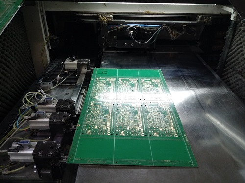
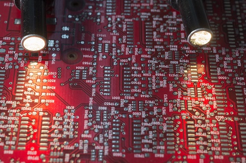
PCBs with thick mosaic layers, the appearance of which is shown in Fig. 1, can be single- double- or multilayer. These PCBs initially found use in aerospace and military industries, where they continue to
serve mainly in power supply, management and distribution systems.


Fig. 1. Examples of PCBs with thick layers of copper foil.
Currently, thick mosaic layered PCBs have found use in many industrial sectors: manufacturing of welding equipment, solar energy panels, various types of power supply/adapter units and high-power converters, power engineering, as well as automotive and railway industries.
Thick copper foil PCBs boast a number of advantages. Copper is an excellent thermal and electric conductor. Hence thick mosaics improve heat transfer along and across the PCB, which reduces damaging stress caused by uneven heating of the PCB. The stress may result in microfracturing of the mosaic, leading to intermittent or permanent open circuits and, ultimately, failure of the affected device.
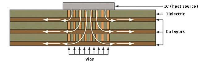
Fig. 2. The heat transfer and dissipation in mosaics
Efficient heat transfer allows installing classic heat sinks directly on the mosaic surface. Another frequent solution has the heat-generating power components on one side of the PCB, while the other side is fully covered with a layer of copper and acts as a heat sink. The heat is transferred between the layers by arrays of vias (Fig. 2.). These methods help reducing the device assembly and manufacturing costs significantly.
Another advantage of thick conductive layers is the increased thermal resistance and current-carrying capacity of PCBs, which results in improved reliability of devices operated in harsh environments, especially at high ambient temperatures. This way the mechanical resistance of contact points and PTH’s is also increased.
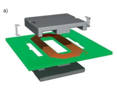
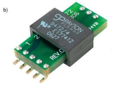
Fig. 3. (a) Cross-section of a planar transformer with double-sided laminate; (b) Overview of a finished transformer module, based on a multilayer PCB.
Another application example of PCBs with thick mosaic layers are miniature planar transformers (Fig. 2), which have been increasingly popular in pulse converters. Unlike typical transformers, the windings are made over the PCB plane as paths in the shape of coils. The windings are arranged around cuts, into which parts of the ferrite core enter, and bound with spring clamps (Fig. 3a) or adhesives (Fig. 3b). This solution enables manufacturing of extremely minute transformers with low winding leakage inductance. The planar arrangement of windings also favours transformer cooling and reduces the Kelvin effect which reduces the power efficiency of transformers.
Design principles
What should be considered first when designing PCBs with thick conductor layers is the processing capacity of PCB manufacturers; it depends on the machines in the processing lines, and the types of chemical etchants at their disposal. The processing capacities define the DRC (Design Rule Check) parameters, which in turn define the minimum permitted dimensions and spacing of, or clearance between, mosaic components. Table 1 shows the DRC parameters for a PCB manufacturer, TS PCB. As shown, the DRC parameters increase directly with the copper foil thickness.
Table 1. DRC parameters vs. copper foil initial thickness.
|
Parameter
|
Copper foil baseline thickness
|
|||
|
105 µm
|
140 µm
|
175 µm
|
210 µm
|
|
|
Min spacing [mils]
|
13
|
15
|
20
|
27
|
|
Min. path width [mils]
|
12
|
14
|
18
|
25
|
|
Loss [mils / mm]
|
ca. 3 / 0.08
|
ca. 5 / 0.13
|
ca. 6 / 0.15
|
ca. 7 / 0.18
|
The process of thick mosaic etching features an effect called ‘undercutting’, where the circuit path width is reduced. The effect is shown in the figure below, which presents a cross-section of a laminate before (Fig. 3a) and after etching (Fig. 3b). The components marked ‘Resist’ in the figure are a protective layer which is a photopolymer in single sided PCBs or tin, deposited at the end of the galvanic coating process, on double and multilayer PCBs. Undercutting reduces the cross-section of PCB paths from square to trapezoid-like.
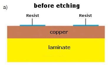
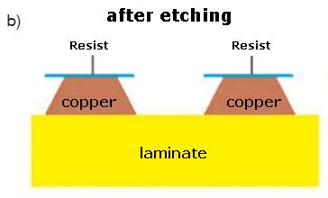
Fig. 4. Cross-section of a laminate (a) before and (b) after etching
When designing multilayer PCBs with thick conductor layers, particular attention must be paid to the copper fill level between the inner layers. If the fill level is too low at a low resin level, the ‘resin hunger’ effect arises and voids appear between the PCB layers, which results in delamination. The negative effects and countermeasures are discussed in detail in a paper by Rafał Tomaszewski, TS PCB process engineer, “Budowa, właściwości i projektowanie wielowarstwowych obwodów drukowanych” (Structure, characteristics and design of multilayer PCBs), featured in the July 2015 issue of the magazine “Elektronik”.
Delamination can be avoided when the copper fill level is at least 75% for the 105 µm or thicker inner layers, whereas the copper distribution must be as uniform as possible. It is recommended to select the types and number of prepregs with software that assists in designing multilayer build-ups, e.g. Multical from Isola or Multilayer Architekt from Technolam.
The following shows the figures of a build-up developed in the Multical tool for low (Fig. 4a) and correct (Fig. 4b) copper fill levels of the inner conductor layers. Reduction of the copper fill level from 75% to 50% results in a drastic loss of the resin fill level by 69%. The actual PCB manufactured with a build-up shown in Fig. 4a features delamination caused by the resin hunger effect.


Fig. 4. (a) Insufficient and (b) correct 140 µm thick copper fill level of inner layers.
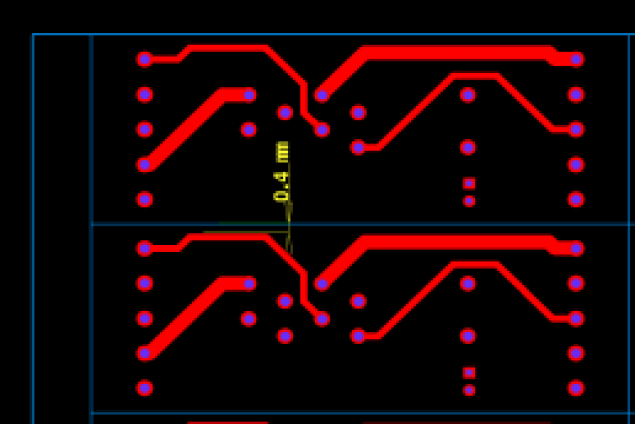
The galvanic coating of PCBs that feature conductor layers over 105 µm thick requires deposition of 40 to 50 µm more galvanic copper than PCBs with thinner copper layers that typically feature 25 µm per galvanic copper layer. The layer improves the mechanical strength of metalized holes (PTH), but it may also reduce the finished diameters of certain vias by more than 0.1 mm, which is a general assumption for thin copper PCBs. The value is assumed as a mean metallisation thickness inside the metallised hole walls and added to the diameter values of the designed holes to determine the drill bit diameter values.
Another consequence of applying thick copper layers is a significant increase in the finished thickness of a PCB, since a soldering resist layer must also be thicker (aside from the copper alone) to effectively protect the mosaic edges. Hence the final circumferential thickness at least 0.25 mm higher than the original thickness.
Summary
This paper presents the characteristics of PCBs with thick conductor layers. The fields of application, design principles and processing limitations of the PCBs are discussed. The information contained in the work helps eliminate the necessary design clarification with customers at the CAM development stage and minimise the production costs of printed circuit boards with constant reliability and quality retained in the process.
Show more from category PCB documentation
-
PCB documentation

Integr8tor - problems solving
-
PCB documentation

Integr8tor—project processing
-
PCB documentation

Automated Analysis of PCB Designs - the process of creating production documentation
-
PCB documentation
How to optimize machining of printed circuits? - part 1
-
PCB documentation

Bridges – structure and parameters
-
PCB documentation

What to remember while designing multilayer PCBs?
-
PCB documentation
Accepted file format for printed circuit board designs
-
PCB documentation
How to correctly design panels for small circuits? - part 2
-
PCB documentation
How to correctly design panels for small circuits? - part 1
-
PCB documentation
Proper preparation of copper layer
-
PCB documentation

Proper preparation of solder mask layer
-
PCB documentation

Proper preparation of PCB outline