
What to remember while designing multilayer PCBs?
Łukasz Romik Author
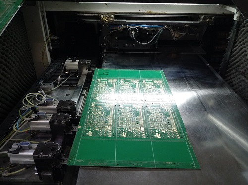
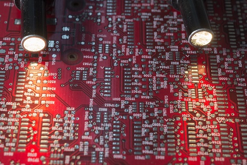
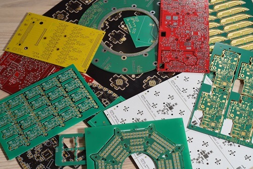
The structure of multilayer PCBs is much more complex than PCBs with one or two copper layers.
Some aspects of their construction should be considered at the designing stage.
Below some general advice is provided to avoid the most common problems, which arise both at production and operation stages.
- specify the layer stackup;
- use at least two prepregs between copper layers;
- stack up layers based on materials available from a given producer;
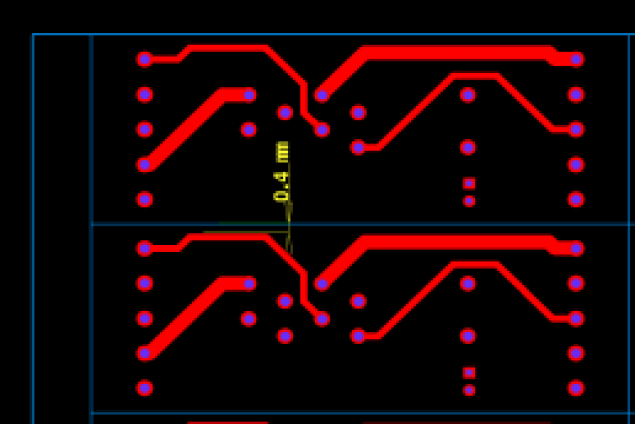
- PCBs with copper thicker than 35 µm on internal layers and on small areas on internal layers require using more prepregs (>2);
- when designing a layer stackup, 10% tolerance for dielectric layer thickness must be considered;
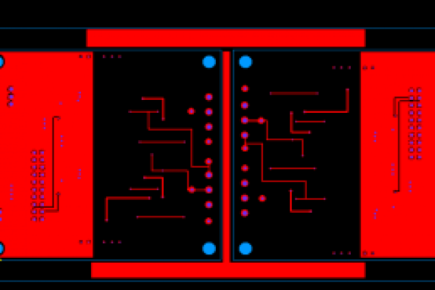
- control DRC parameters on internal layers as well – in particular annular rings width;
- if feasible, fill empty internal layer areas with additional non-functional copper;
- use teardrops between pads and traces (internal layers);
- remove non-functional pads on internal layers;
- copper layers and dielectric layers should be symmetrical in relation to the PCB centre.
Show more from category PCB documentation
-
PCB documentation

Integr8tor - problems solving
-
PCB documentation

Integr8tor—project processing
-
PCB documentation

Automated Analysis of PCB Designs - the process of creating production documentation
-
PCB documentation
How to optimize machining of printed circuits? - part 1
-
PCB documentation

Bridges – structure and parameters
-
PCB documentation
Accepted file format for printed circuit board designs
-
PCB documentation
How to correctly design panels for small circuits? - part 2
-
PCB documentation
How to correctly design panels for small circuits? - part 1
-
PCB documentation
Proper preparation of copper layer
-
PCB documentation

Proper preparation of solder mask layer
-
PCB documentation

Proper preparation of PCB outline
-
PCB documentation
PCBs production documentation – how is it created and what are its contents?