Impact of laminate parameters on the life and performance of printed circuit boards
25.11.2015
The life (or durability) and reliability of electronic equipment depends on the quality and types of applied components, including the printed circuit boards (PCBs), which are the cornerstone of a performer electronic circuit. Hence it is extremely important to properly select the parameters of base laminates for long life and reliable performance of finished products.
Currently the PCBs are manufactured with laminates on the following substrates: glass-reinforced epoxy (designation FR4), aluminium MCPCB (Metal Core PCB), Teflon, or ceramic. The laminate type selection depends on the application of the finished device and its operating conditions. This article largely focuses on the parameters of FR4 glass-reinforced epoxy laminate, since this type is the most popular. Other material groups will be referred to by comparison to discuss certain parameters.
Basic parameters
Thickness is a principal parameter characteristic of every PCB. Thickness is the total thickness of base laminate, i.e. copper foils and the dielectric material and the in-process deposited coats (from metallizing, soldering resist, and gold or tin plating). This means that the finished laminate thickness is always greater than the base laminate thickness.
Electronic devices often have special enclosures with snap closures or aluminium guides for mounting of PCBs, hence the finished tolerance requirements for the PCBs are restrictive. The PCB thickness tolerance include the thickness spread of the dielectric material and Cu films.
Their permissible thickness tolerance is defined in IPC 4101, which distinguishes 3 possible thickness spread intervals. The laminates of the highest class, C/M, feature the narrowest tolerances and guarantee high repeatability and quality of manufactured PCBs. Class C/M laminates are used by many manufacturers, including TS PCB, since the PCBs produced with them are highly reliable.
When ordering designs with a specific tolerance for the identified laminate thickness, ask the PCB manufacturer for assistance, who will choose the optimum laminate type and structure. It is important to clearly define whether the expected thickness value is for the base laminate or the finished laminate. Mind also that if the tolerance is not specified, the PCB manufacturer will deliver their standard tolerance.
Another laminate parameter that defines the breakdown strength between the circuit paths in wet ambient conditions is CTI (Comparative Tracking Index), expressed in volts (V). There are 6 PLC (Performance Level Categories of this parameters (see Table 1, where PLC3 is a standard of many PCB manufacturers.
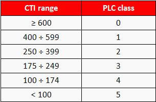
Table 1. CTI class
The higher the PLC is (with PLC0 being the maximum) for a laminate the safer use of the device will be. High CTI values are particularly important in high-voltage equipment that are in direct contact with humans or operated in high humidity conditions.
The highest safety of use is guaranteed by laminates with the UL Certification monitored by Underwriters Laboratories and specifying the flammability of materials. High quality laminates with the highest UL class are designated with the symbol "94V0". Those PCBs must be produced by manufacturers who have their manufacturing processes UL-certified; only the will the finished PCB exhibit fully UL-compliant burn resistance, or non-flammability.
Temperature parameters
Thermal overloading of laminates may result in parameter or permanent failure. Protection from damaging overtemperature effects requires laminates with the thermal performance adjusted to the assembly process and the target device operating conditions. The following presents the most critical factors which determine the thermal characteristics of laminates and which should be considered by designers who selected the base laminates.
The factor Tg defines the so-called 'glassy temperature' at which the mechanical properties of the laminate are drastically reduced. This is caused by transition of the laminate structure from its glass (hard) state to a plastic (soft) state, simultaneous with a rapid increase of the laminate expansion in the Z axis. When this temperature limit is exceeded, the mechanical loads acting on the affected PCB will usually lead to permanent deformation and delamination (see Fig. 1), accompanied by reduced adhesion of the mosaic and lifting of the copper foil.
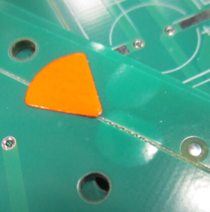
Fig. 1. Example of delamination.
The factor Td is the chemical decomposition temperature of laminates. The standard IPC 4101 defines the parameter as the temperature at which the affected material loses 5% of weight. The parameter T260/288 denotes the delamination time. This is the time for the delamination to occur. The time is measured when the laminate reaches 260°C or 288°C.
The parameter CTEZ,XY (Coefficient of Thermal Expansion) is the coefficient of thermal expansion of laminates that is projected along the XY plane and the Z axis. The CTE increases significantly above the temperature Tg, and the laminate begins to swell rapidly. This factor is extremely critical to the laminate performance at high temperature; the expansion of laminate in the Z axis results in stresses of the conductor at vias, the negative impact of which is the lifting of pads and cracking of via edges (see Fig. 2) or via holes. The usual result is a defect of vias consisting in the formation of open circuits. The electrical continuity across the vias may be restored intermittently, e.g. when the laminate operating temperature is reduces or mechanical forces are active.
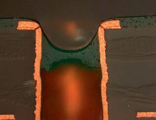
Fig. 2. Cracking of via hole edges.
The discussed negative effects of laminate overheating can be avoided by selecting the right laminate type at the design stage so that the MOT (Maximum Operating Temperature) of the assembled pack is not exceeded during the finished device operation. PCB manufacturers recommend production from laminate types the design MOT of which is ca. 15 to 20°C lower than Tg.
Table 2 shows the relationship between Td, CTE and MOT vs. Tg. When the Tg and Td values rise the laminate resistance to thermal stress also rises, both during soldering and further operation. S CTE values reduce the risk of stress on vias and of via damage which is critical in PCBs with a via diameter below 0.2 mm. CTE can be lowered by increasing Tg.
Thermal expansion of laminates is also significant to the development of stresses between the resin and its glass fibres. If the forces that bind the resin with the glass fibres cannot counter the increasing temperature related stress, delamination occurs and the risk of CAF (Conductive Anodic Filaments) increases (see details in "Elektronik" issue 8/2014).
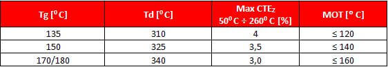
Table 2. Temperature parameters at various Tg values.
Table 3 shows the recommended thermal class of the applied laminate in relation to the laminate thickness and projected soldering cycle count. It is evident that the currently commonplace laminates with low Tg values are bound by large restrictions; for example, their permissible soldering cycle count is 3. Note that HAL tin plating of circuits is tantamount to one soldering cycle, since the temperature of the tin alloy bath is 280°C. This means that the assembler will have only two soldering cycles left.
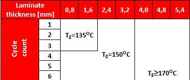
Table 3. Soldering cycles vs. laminate thermal class.
Increased complexity of designs imposes more strict requirements for laminate classes. This is why laminates of moderate and high Tg values have seen increasing usage; they resist much greater thermal loads during PCB assembly and finished device operation. These laminate types minimise the risk of circuit failure during rework, repair or servicing.
There are conditions under which the heat generated by the PCB components is high enough not to be effectively dissipated by traditional methods. One of the restrictions is the laminate TC (thermal conductivity), which defines the efficiency of heat transmission to the environment and reduction of heat retention within the material. This effect forces the assembly of high-power circuits or LED systems on aluminium MCPCB the TC of which may reach as much as 5 W/mK. A tell-tale comparison: the thermal conductivity of the standard FR4 laminate is 0.4 W/mK.
Humidity absorption
Humidity is one the most damaging enemies of laminates. According to IPC 4101C, the parameter must never exceed 0.8% in the material. Excessive humidity absorption reduces the laminate performance parameters (e.g. Tg), increases the risk of CAF and the risk of defects during thermal processing, such as delamination.
Proper storage conditions of PCBs help reducing humidity absorption. PCB without vacuum sealed containers should be stored at 17 to 23°C and the maximum RH (relative humidity) must never exceed 50%. Vacuum-packed PCBs are at no risk of humidity exposure as long as the container remains sealed. Still, the storage temperature of packed laminates is important.
Proper storage conditions are particularly critical when PCBs must be shipped to distant destinations, especially by sea, or whenever other risks of humidity exposure arise. Special humidity indicators and desiccants are used in those cases. A temporary solution that reduces humidity is to hold PCBs (especially the multilayer types) at elevated temperature directly before assembly.
Electrical properties
When considering a laminate versus the frequencies present in the designed circuit, two basic parameters should be followed: dielectric constant Dk and lossiness Df.
Dielectric constant defines the relative permittivity of materials to vacuum. The higher the value is, the weaker is the electrical signal. The standard FR4 laminates exhibit high dielectric constant values (above 4), and the parameter largely depends on frequency, which disqualifies those materials for high frequency applications. High frequency systems demand Dk<3.9 at 2 GHz and with small variations of the parameter in a wide frequency range.
Lossiness Df defines the signal loss caused by absorption into the material followed by conversion into heat. The lossiness at 2 GHz should be less than 0.01. Signal losses can be avoided by applying laminates with the lowest Dk and Df values, and based on Teflon or ceramic substrates.
The standard FR4 laminate is intended for assembly of PCBs operated up to 0.5 GHz. However, special versions of FR4 exist, e.g. Isola FR408 with frequency parameters better than the typical glass-reinforce epoxy laminates. Laminates designed for operation in the microwave range are based on ceramic dielectric materials (e.g. Rogers RO4003) or Teflon (e.g. Rogers RO3003). Another advantage of these laminates is their high Tg of 280°C.
Another parameters that defines the electrical properties of laminates is the dielectric breakdown strength, a feature important in high voltage systems or systems that require special insulation of individual copper layers, as in multilayer PCBs. Here the typical values range from ca. 40 to 50 kV for the laminate thickness ≤ 0.5 mm (as tested according to IPC-TM-650 clause 2.5.6). The aluminium laminates, which feature significantly thinner dielectric materials (usually at 125 µm), the breakdown voltage is 2.5 to 3.0 kV.
Summary
The work presents the essential parameters of laminates. Their understanding will allow design engineers to select the best optimum laminates for the specific requirements and operating conditions of target equipment. It is enough to apply high quality laminates offered by leading manufacturers, e.g. TS PCB to assure long life and failure-free operation of devices.
Albeit somewhat more expensive than the typical variants, it is more cost effective in the long term to suffer greater production costs of better PCB classes than much higher costs of extra servicing and repairs of the equipment damaged by incompatible laminates.