Solder masks in printed circuits - application process
The solder mask (wet) is applied to the surface of the circuits using two methods: screen printing and photo printing.
Screen printing consists in applying the mask image by means of a screen and then hardening it thermally or with use of UV radiation.
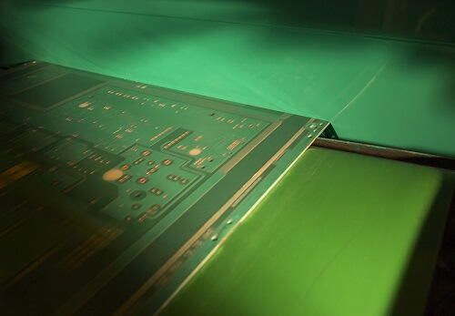
In the photo printing method, paint is applied to the entire area of the board — e.g. curtain (photo 1), and then expose the image through photographic film by using UV radiation. The applied paint can also be developed with use of a direct imagesetter, making the use of film unnecessary. It is a precise yet time consuming method of exposure because the currently masks and their thickness require a large amount of energy for their full exposure. In both cases final hardening of the coating is achieved by heating in an oven at a high temperature and specific time.

Photo 1. Applying the curtain mask.
The solder mask is applied to copper previously subjected to a micro etching process to increase its adhesion. Its function precludes it covering areas involved in the assembly of components, which in the next stage of production are protected by a selected type of coating (tin, chemical gold, silver, etc.). The exposures can also be used for making additional markings — e.g. inscriptions — although bearing in mind that placing them in the copper areas will lead to their permanent exposure and the application of the cover.
It is worth remembering that the width of the demaskings, especially for the popular HAL tinning method should not be less than 15 mils. Otherwise selected demaskings may not be completely tinned, exposing bare copper which may attract corrosion.
A peelable mask is applied to ready circuits so as not to damage them during the other processes. As mentioned, it is applied by using the screen printing method and then heated in an oven. In the absence of additional guidelines, the peelable mask is prepared for the standard soldering process which may be too dry for a long-term or multi-stage assembly. In such a situation, the mask layer may be difficult to remove — it will dry up as a result of long exposition to high temperatures and will crumble when removed. On the other hand an undried coating will leave greasy marks on the surface of the solder fields.
Check also: Solder masks in printed circuits - types and basic functions