Solder masks in printed circuits - designing
Masks are prepared as negative layers so any components placed on them will in fact be areas free of paint. Typically these are SMD pads or assembling holes which can be defined in two ways (fig. 1):
- by copper which means that the mask does not influence the pad size — the opening is larger than the pad,
- by the mask which means that the mask area influences the pad size — the opening is smaller than the pad.

Fig. 1. Pads defined a) by the copper, b) by the mask.
Such a distinction is usually found in relation to assembly pads of BGA systems. The choice of method depends mainly on the manufacturer recommendations of a given component. However, it is recommended to use, as far as possible, the pads defined by copper because they ensure a more reliable diameter adhesion — the connection is also made on the side surface of the pad. Thus, the pad diameter can be smaller than the BGA lead diameter thereby increasing the space for conducting the paths. Another advantage is the increased precision of the soldering point position, which in the case of defining by the mask can change its position and dimension due to the lower accuracy of the anti-solder masks in relation to the mosaic mapping. The introduction of the IPC standard allows for minor overlapping of the mask on the pads although it is desirable to maintain proper openings. For this purpose, they should be enlarged in relation to the corresponding mosaic pads in order to compensate for its possible maximum displacement. Renowned manufacturers of printed circuits increase the openings on their own to adapt them to their own production process. Therefore, the designer does not have to worry about this element during the PCB design.
The advantage of pads defined by the mask is their increased resistance to the so-called pad lifting phenomenon — i.e. pads tear away from the laminate because of high temperature or mechanical stress, which does not take place while maintaining the correct specifications of the components’ assembly process. This is due to the larger pad surface which ensures greater resistance to detachment from the dielectric. In the case of systems with a small raster (0,4 mm or less), the possibility of bridging the pads with tin is also limited.
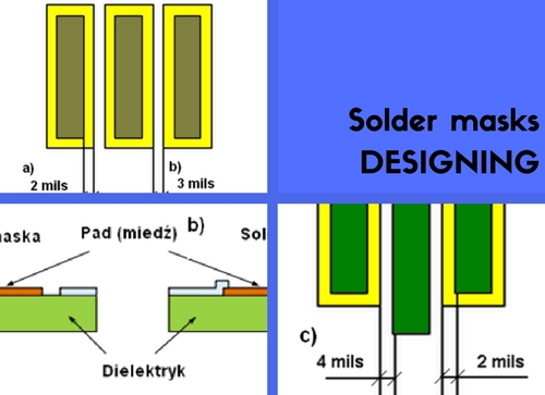
There are three main specifications which characterize the geometry of the mask layers:
- increasing the demasking of the mask in relation to the pad (a);
- the width of the bridge from the mask between the pads which is equivalent to the minimum distance of adjacent demaskings in the absence of paths between them;
- the width of coverage with a mask between the path/mass and the adjacent demasking which is equivalent to the minimum distance of the adjacent demaskings when there is a path between them.


Fig. 2. The solder mask design specifications.
Fig. 2 presents the recommended minimum mask specifications used among others by TS PCB — a producer of printed circuits from Gdansk — for masks exposed with a film. A higher resolution can be obtained with direct exposition — e.g. by reducing the magnification of the pad demasking by up to 0,5 mils. The presence of mask bridges between the soldering pads of microprocessor systems is often required to perform a correct assembly. Therefore, at the design stage it is worth ensuring the minimum width of the mask allowed by the printed circuits manufacturer.
Check also: Solder masks in printed circuits - types and basic functions