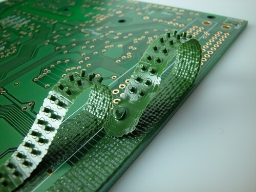
Solder masks in printed circuits - performance specifications

The specification most often charactering the mask’s performance is it thickness.
In the case of a wet mask, it is a maximum of 40 µm ÷ 50 µm (thickness in mass areas) assuming that it is applied to copper with a typical thickness of 35 µm. The mask has a tendency to run off the paths edges and so its thickness is the least in those places and is usually 7 µm.
Unfortunately, in case of thick copper layers (over 70 um), galvanically applied copper creates a characteristic ‘mushroom’ on the paths (extending above the photopolymer layer) making it difficult to cover their edges in a such way as to meet the requirements of the IPC standards. It is then necessary to apply a thicker layer of paint (e.g. twice) while also increasing the maximum thickness of the mask on the mass areas.
The most often used solder mask colour is green with an emphasis on matte rather than glossy types which reduces problems during assembly (reflections, poor contrast).
Due to its popularity, it is relatively cheap, ensuring a good contrast between the copper and the laminate which facilitates visual inspection. The use of other colours is for purely aesthetic reasons — to give added value to the final product. There are, however, some exceptions —e.g. white — whose properties associated with high reflectivity are used for the production of circuits for the LED lighting industry. However, their disadvantages include:
- longer exposure time;
- risk of the colour tone distorting under the influence of a high temperature or chemical agents.
- smaller resistance to the action of chemical agents, e.g. washing;
- more difficult to assemble.
Black is another possible mask colour. Glass-epoxy laminates (most often used in PCB production) are relatively transparent. In order to limit their transparency (as well as light reflections) black anti-solder masks are used. They also provide a good contrast (background) for LED displays. The disadvantage of a black mask is the accentuation of all imperfections, soiling and damage — e.g. dust and scratches.
The solder mask also covers the rings and inside of the metalized holes, which is also referred to as tenting. It is possible to clog the grommet with the mask in such a situation but this is not guaranteed. This is most often possible for grommets of small diameters (≤0,3 mm). It should be remembered that the paint is applied on the circuit with an even layer so in the location of the holes its thickness will be less than the flat areas due to the material flowing into the holes. Although, resistance for tin intake is ensured, electrical insulation, assuming direct contact, may be suffice. This may then lead to the breaking of the grommets' insulation barrier placed usually under the integrated circuit in the SMC enclosure with direct contact with it terminals. In this situation the following solutions may be applied:
- covering the circuit with two mask layers — not always possible and incurs additional costs,
- covering sensitive pads with descriptive paint — when the design provides descriptive layers, such a solution does not generate additional costs,
- fill the grommets (clog) and cover with the mask — this operation features an additional charge but is the most effective.
Beside ensuring the correct thickness of the mask layer on the grommet rings, the above solutions additionally protect the holes against solder penetration and, in ready devices, provide an environmental barrier restricting moisture penetration.
Check also: Solder masks in printed circuits - types and basic functions


