Standard structure, non-standard application of PCBs
With the use of typical elements, such as tracks and metallised holes, one can realize more complex technological solutions on the surface of a printed circuit.
The first atypical application of the printed circuit, which is worth mentioning, is the creation of integrated modules that are surface mounted directly to another printed circuit. The exaples can be widely used Wi-Fi, and Bluetooth modules or GSM, and GPS modems.
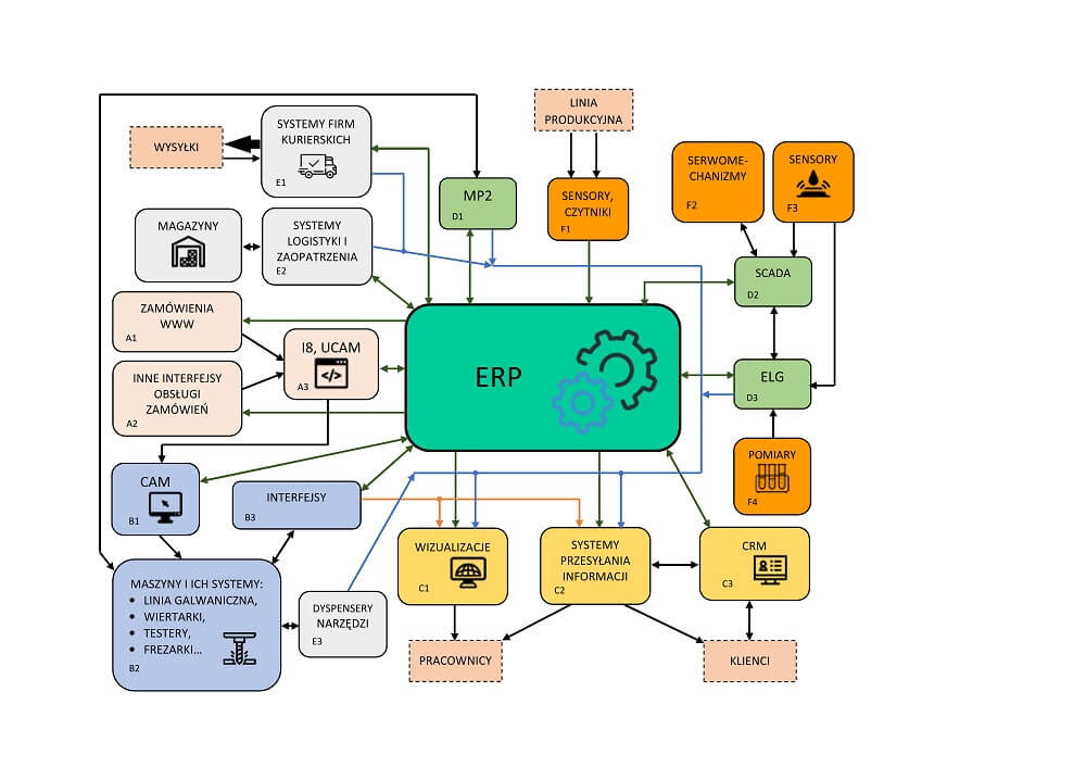
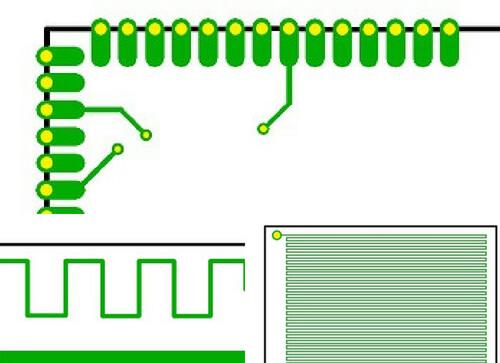
In the same way, you can also design adapters for integrated circuits, allowing PCBs to be mounted on elements with a different pin layout or housing, without the need to design a newer circuit version. The easiest way to mount such a module/adapter is to use metallised castellated holes, which act as contact fields (Fig. 1). This solution can also be used to connect two PCBs, also at right angles, in order to eliminate cable connections.
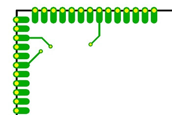
Fig. 1 Example of a project with the castellated type assembly holes
Another example is building planar transformers in the structure of the printed circuit. Unlike typical transformer, the windings are made on a layer of copper in the form of flat coils. Inside, holes are made through which the cores pass. These types of structures are characterized by small dimensions, low profile and good operating parameters (very good thermal parameters, low leakage inductance, constant operating parameters). They can be constructed as elements integrated into the printed circuit (fig. 2A) or stand-alone components of the multi-layer structure (fig. 2b).
(a) (b)
Fig. 2 Example of a planar transformer construction (left) and a view of a complete transformer module (right)
In the mosaics of printed circuits, you can also design various types of antennas, so-called microstrip antennas with radiators in the form of tracks or in the shape of a rectangle. The first highlighted type is the so-called integrated meander-type antenna (Fig. 3), which is a component of the printed circuit board (the structure is created in a separate circuit area).

Fig. 3 An example of a design with an integrated antenna
Its advantage is the lower cost in comparison to the antenna assembled as an external module because its price is basically the price of PCB and it also eliminates the need for additional assembly. Thanks to the ease and precision of production e.g. by etching, you can individually tune up its performance, e.g. impedance, standing wave ratio, and limit the signal loss.
The technology is used to build panel, Yagi-Uda type directional, reversed F-type branched, and helical antennas, such as those for 2.4 GHz (WiFi, Bluetooth) bandwidth applications.
The antenna can also be made as a separate element with an area of the entire printed circuit. However, regardless of the way it is made and the degree of integration it is important that the material on which the antenna is made ensures its proper operation. Most often, the integrated antennas, due to the size of mosaics as well as the thickness of laminates, work mainly in the band from hundreds of MHz to single GHz.
Copper tracks on the plane of the circuit board can also be formed in such a way as to act as a heater (resistance heater, figure. 4).

Fig. 4. An example of resistance heater
It can heat a fluid either directly – by immersion or putting a vessel on the heater, e.g. as a mug heater. These types of heaters are also used to heat the substrate (heating table) in 3D printers.