Unusual applications of printed circuit boards and laminates
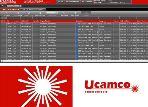
A printed circuit board is most likely defined as copper track layout placed on both sides of the dielectric substrate, connected by appropriately located metallic through holes (Fig.1).
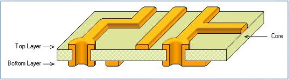
Fig. 1
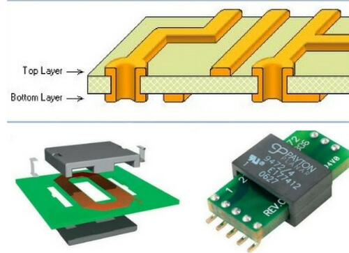
Its essential features are especially durable and accurate representation of connection network, while providing surface for mounting components, leaded at first, and now mainly surface-mounted (Fig. 2).
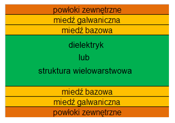
Fig. 2 Typical PCB structure
The present, fast-progressing development of electronics and the accompanying miniaturization also pose higher and higher demands on electrical and mechanical parameters of PCBs.
The tasks of printed circuits are, therefore, not only permanent mapping of electrical connections but also, among other features, low signal loss, possible high breakdown and leakage resistance, high mechanical durability and reliability when working in high temperature or aggressive environment.
These expectations forced the improvement of the production technology of circuits, and the production of laminates with desired characteristics. Over the years, it turned out that materials used for the production of printed circuit boards can also be successfully used in other applications.
Printed circuit board manufacturers can now create even very complex structures of the copper layers and dielectrics, with high precision. Modern technology allows production of hybrid circuits consisting of typical FR4 laminates and materials with Teflon or ceramic substrates, dedicated to high frequency applications. These solutions allow materials of different properties to be integrated into one structure. Thanks to the aforesaid the PCB and the device itself are more compact and reliable. The production cost is lower compared with the implementation of separate systems working with signals of high and low frequencies.
In addition to a wide selection of laminates themselves, the designers have a variety of technologies at hand, for advanced mechanical processing:
- milling complex shapes, notches and slots,
- depth milling,
- hole and edge bevelling.
In order to increase the aesthetic values of the circuits themselves, they can use colored anti-soldering masks and descriptive layers – both on the entire surface and freely designed patterns in selected areas of the perimeter.
It is evident that in addition to the typical role of the printed circuit (implementation of electrical connections), typically mechanical and aesthetic functions gain in importance.