How to prepare a good production documentation, or what design engineers must know when working with PCB manufacturers
25.11.2015
The cooperation between the PCB designer and the PCB manufacturer is extremely critical. The better the first order delivery stage is prepared, the shorter is the time to receive PCBs that meet customer's specification. A production documentation that is vague or unclear will extend the time to production launch. Clarification of all doubts requires more interaction, both from the manufacturer and their customer.
The following article presents the standards for production documentation delivery to PCB manufacturers, rules for good design development, and a presentation of the most frequent errors found in the production documentation. This information is based on the experience of CAM engineers employed by TS PCB. It will certainly aid design engineers in the areas of PCB quality and reliability, and may also reduce the PCB production costs.
File formats
Gerber is the general standard of PCB production documentation. The standard allows saving vector images of design layers: mosaics, masks, text, etc. Two versions currently exist: the older Standard Gerber RS-274D and the modern Extended Gerber RS-274X.
The RS-274D has become obsolete and is now rarely used. The files in that format contain only the coordinates of layer image components and does not define the applied apertures. PCB manufacturers require a list of applied apertures to properly process RS-274D designs. The newer and most popular version, the RS-274X has no drawbacks of the RS-274D. The layer files in this format contain the complete data required to process PCB designs, i.e. the coordinates with aperture definitions.
The machining parameters (i.e. drilling and milling/routing) are most often saved in the Excelon format version 2. A complete program for CNC drilling and milling/routing should define the applied tooling diameters in the header. It may also keep the information about the notation format for coordinates and units of measure. This may speed up the design processing by the PCB manufacturer.
The most popular PCB CAD software products (e.g. Altium Designer, Eagle, and Protel) support export of the design documentation in the above formats. Most PCB manufacturers prefer Gerber RS-274X and Excellon2, but other data set formats can be accepted: RS-274D, Dynamic Process Format *.dpf, GraphiCode GWK, ODB++, and BRD (Eagle).
Features of a good design documentation
From the PCB manufacturer's perspective, a well-developed design contains explicit data that raises no questions and meet the processing capacities. The following lists a set of recommendations for PCB designers, grouped in five general themes.
DRC
.JPG)
Fig. 1. Areas non-conforming to DRC parameters.
There is a sporadic design error that may hamper or prevent a PCB from being produced is the exceeded DRC (Design Rule Check) parameters. DRC parameters determine the processing capacities of PCB manufacturers, i.e. the minimum permissible width of mosaic components (i.e. paths and text), their spacing and the hole ring sizes. The majority of popular PCB CAD programs have configurable DRC's to control compliance of designs with manufacturer's predefined capacities.
The design of a PCB mosaic must consider that all narrow cuts on mosaic surfaces are extremely hazardous (see Fig. 1). These areas must be filled, since the minimum permitted clearance rule also applies to the mosaic parts within the same interconnection network. The DRC parameters apply to the text deposited on copper layers. Too small characters might be digested by etching and become illegible.
Outline
Fig. 2. View of a mosaic layer: (a) component side; (b) soldering side.
The PCB outline must be located on a separate layer and be formed as a closed envelope that is free from offsets relative to other layers. The outline must also feature the forms and locations of all cuts and slots that need to be processed. The outline layer can feature marking of the PCB dimensioning, including the tolerance specifications (if different from the defaults applied by the specific PCB manufacturer).
The outline and cuts are often located on the layers of text, solder masks or mosaics. There is a risk then that a CAM engineer may overlook the cuts and their production will fail. Problems also arise when the PCB forms are shown on several layers and contradict one another.
Text layers
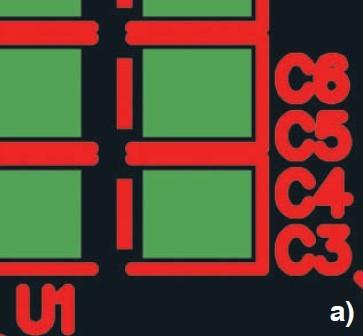
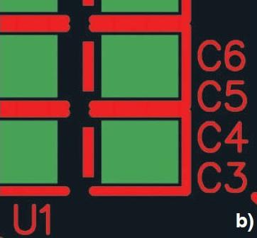
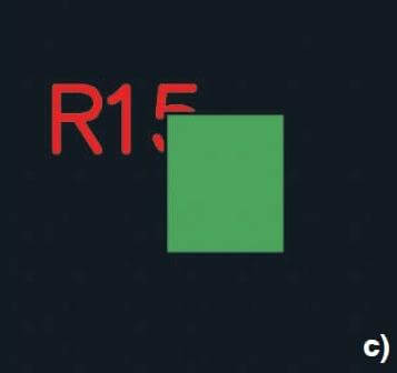
Fig. 3. Text line thickness vs. text quality: (a) 0.25 mm line text; (b) 0.1 mils line text; (c) a text cut by an SMD pad.
A common error is the incorrect development of the text layer that renders the markings illegible and incomplete. Good legibility of text requires proper character height and text line thickness. The optimum character height is from 1 mm up. The minimum text line thickness is 0.1 mm. If a text line that is extremely thick relative to the character height, legibility and clarity of text can be improved by reducing the text line thickness (see Fig. 3a & 3b). The solution improves the aesthetic value of the PCB and facilitates assembly of components. Design engineers should never locate any markings on the soldering points or holes in the PCB design. PCB manufacturers remove text from pads and other unmasked circuit areas by default (see Fig. 3c), because ink on soldered components prevent correct assembly. The loss of text by trimming can be reduced by applying a minimum clearance of 0.1 mm from the pads exposed in the solder mask and the holes.
Machining
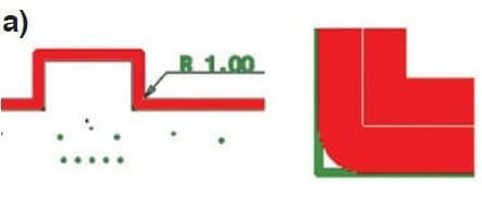
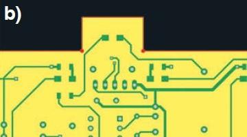
Fig. 4. Preparation of cuts in a PCB: (a) with the standard 2 mm dia. mills; (b) cut diameter reduction.
It is critical to properly prepare and label the holes and slots on the PCB board. One CNC drilling program can feature the boring of PTH (Plated Through Hole) and NPTH (Non Plated Through Hole) openings and slots. It is also important to mark the hole types than can be manufactured. This is done by adding comments in the single drilling program or an additional informative file. The PTH can be separated from the NPTH into two individual drilling programs with proper names. A common practice is to deliver the drilling map on a separate design layer. If no other information is specified, the PCB manufacturer will follow the layer to properly define what holes are PTH or NPTH. All single-sided holes are deemed NPTH.
The specified diameters are always understood as target, unless the order specifies otherwise. This means that the PTH and NPTH diameters in a finished PCB will be equal to the diameter values specified in the drilling program header.
The drilling programs for blind and buried vias must be enclosed in separate files, i.e. not in the pass through holes and separately for each processing depth. It is also necessary to mark the blind via drilling depth, e.g. by specifying which layers are to be connected.
Milled/routed forms must consider the limited precision of cutting, and the parameter depends on the mill diameter. This causes a problem shown in Fig. 4, i.e. the round-off in the milled form corner. This can be eliminated by locating small diameter processing holes in those corners. The holes may slightly interfere with the PCB surfaces, but they also greatly reduce (or completely eliminate) the round-off radii from the mill pass (Fig. 4b).
Design engineers should keep proper spacing between the mosaic and the PCB edges and cuts, since machining of PCBs has a defined tolerance. Milling, routing and scoring (v-cutting) may damage the mosaic details that are too close to the PCB edges. Not only do the resulting torn copper parts reduce the aesthetic value of the PCB, but may also cause shorting in the assembled device due to accidental contact with the metallic enclosure.
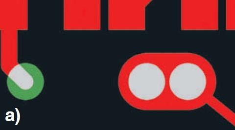

Fig. 5. Slot: (a) with incorrect marking and (b) with correct marking on the PCB outline layer.
Blinded cuts in PCBs that are z-routed must be clearly illustrated in a separate drawing, on the PCB outline layer or on a separate layer altogether. It is also required to specify the side of the PCB and the depth of z-routing. Analogically, the presence of plated edges must also be shown. A very common and proper way of showing plated edges in the design is to located copper areas that extend beyond the PCB outline on the mosaic layers.
PTH slots shown as two adjacent holes (see Fig. 5) may also be doubtful during the design documentation development. Every designer should be aware that CAM engineers who prepare the designs for production usually do not know which components are assembled on specific PCBs. It is unreasonable to expect that 2 adjacent holes, shown in Fig. 5a, will be construed as a PTH slot. In this case the slot must be properly marked on the PCB outline layer (see Fig. 5b).
Layer file development and names
The images of individual layers must be generated to identical scale and without offsets. The hole layer can be offset relative to other layers, but note that it is not always possible to properly align the layer with the other ones. A common standard is to arrange the layers in a view from the PCB top side. This means that when a design is loaded in PCB CAM software, all text on the component side of the layers are legible (see Fig. 2a), whereas the texts on the mosaics, solder masks or the soldering side will be seen mirrored (see Fig. 2b).
It is good to use layer file names and/or extensions that can be easily interpreted. The file nomenclature is usually defined in the PCB CAD software. Aside from generating the Gerber and Excellon files, the majority of such applications can also output and additional text file (i.e. a report statement) with the list of export output files and the specification of the applied notation of coordinates and units.
Multilayer PCBs require providing the specification on the sequential order of the inner layers. The sequence can be specified by numbering the layers directly or proper file nomenclature (e.g. *.L1, *.L2, *.L3, *.L4, etc.). The information can also the provided in the PCB processing sheet.
Placing several processing components on a single layer makes interpretation of the documents very difficult. The most common error here is to set a peelable mask on solder resists. Each mask is deposited at a different production stage and thus each requires a separate production documentation.
Summary
A designer's attention to details, knowledge of proper documentation development principles and awareness of specific PCB manufacturer limits of processing directly affect the quality and labour intensity of design delivery. The time spent on configuring the PCB CAD software and thorough circuit design will be rewarded with reliable PCBs that meet designer's expectations, and short lead times.