Methods of printed circuit board pricing optimisation
25.11.2015
 comments (1)
The design of printed circuit boards (PCBs) can be defined as a process of seeking the best layout of the connection networks for circuit components and electronic devices while retaining the desired levels of electrical parameters, e.g. impedance of differential transmission lines, thermal parameters (e.g. proper heat dissipation from SMD power components) and mechanical parameters (e.g. attaining sufficient rigidity at the given material thickness). The final design released for production is not always price-optimised. Prices are generally products of design production complexity.
This article presents the most significant PCB parameters that condition the prices of solutions with example methods for price reduction. The information contained herein has been prepared from the experience and processing capacities of TS PCB.
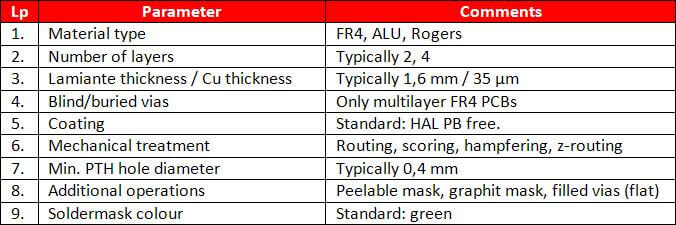
Table 1. Printed circuit processing parameters as extra costs generators.
Table 1 shows the 9 most important price-defining PCB processing parameters. They are arranged by the severity of effect on the finished PCB price. As seen in the table, the key effect on the PCB price is delivered by the material type, which also predetermines the manufacturing process.
Material type
FR4 (see Fig. 1a) is the most popular and cheapest laminate. It boasts universal electrical parameters, i.e. the typical dielectric constant is 4.5, the standard lossiness is 0.02 and the thermal conductivity of ca. 0.4 W/mK are sufficient for the majority of applications. Aluminium core laminates (see Fig. 1b) have much higher thermal conductivity that oscillates at several W/mK, which makes them a popular choice for high-power SMD circuits which are used mainly in the LED lighting sector. Circuits with moderate power losses are recommended to feature the FR4 laminate, because even with thick Cu foils it is more cost-efficient than aluminium laminates, e.g. due to machining costs.
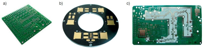
Fig. 1. Examples of PCBs printed on the following laminate types: (a) FR4, (b) ALU, and (c) Rogers.
Teflon-based laminates from Rogers (see Fig. 1c) exhibit low lossiness and are intended for HF circuits. However, they are not always necessary. Systems operated at moderate speeds timed up to single GHz figures can be produced cheaper by using FR408 laminates (from Isola) which have the lossiness of 0.009 at 1 GHz. Other advantages of those laminates is the workability that is similar to that of FR4, and the capacity to build multilayer PCBs intended for fast digital circuits.
Another PCB price relevant parameter is the number of layers, which – when reaching six or more – can significantly increase the purchase cost of PCBs. While cutting two layers to one is not economically rational, building a 6-layer PCB network across 4 layers only will measurably reduce the PCB price. Higher density interconnections require redesigning the mosaic to meet the permitted DRC (Design Rule Check) parameters with the given circuit technology. Moreover, blind and buried vias can be used without a risk of price increase. A 4-layer PCB with blind and buried vias will be still less expensive than a 6-layer solution without the vias.
Laminate thickness
Another factor that defines the PCB price is the thickness of the laminate and Cu foils; the standard values are 1.6 mm and 35 µm, respectively. While production of thinner PCBs (especially single and double-sided types) causes little difficulty, thick laminate circuits (ranging from 2.4 to 3.2 mm), also with thick Cu foils (70 to 140 µm or more) is more complex which inflates the product price.
The price can be minimised by using laminates and copper foils with standard thickness values, if possible. It is possible that maximising the mosaic components to the minimum permissible DRC value may allow the typical 35 µm Cu foil with the permitted current density retained. Another method of increasing the path thickness without using thicker Cu foils is to remove the resists and tin plate; this process increases the thickness by 20 to 40 µm (see Fig. 2).
Fig. 2. Path cross-section increased by tin plating.
Vias and pad plating
Another price-boosting parameter of multilayer PCBs is buried and blind vias. Note that their use may result in additional processing limitations, e.g. the dependence of Z axis penetration depth to via diameter, and thus require switching to chemically deposited gold plating, which will further increase the PCBs price. A more cost-effective solution would be to build all vias as PTH's (Plated Through Holes), if the circuit surface area can be slightly increased.
Pad plating is another parameter that contributes to the finished PCB price. The standard plating is applied by lead-free tin plating with the HAL process (Hot Air Levelling), which should be applied whenever possible to reduce the PCB price. Tin plating is not always permitted. More complex PCBs with minimum DRC values and comprising BGA (Ball Grid Array) encapsulation must be gold plated, and the price relies most often on the plating surface area. In order to prevent unjustified plating price increase, the design should feature most of the vias under soldering resists, and leave only those vias unmasked which must remain accessible for e.g. measurements during functional tests of the pack.
Machining
The machining parameter are also important pricing conditions. This fact is often neglected by design engineers, hence the issue of machining deserves more insight herein. Milling allows production of nearly all PCB forms with the dimensional tolerance of ±0.05 mm.
The processing time and impact on the PCB price grow drastically and inversely with the diameter of mills assumed in the design //URWANO// as the standard 2 mm dia. mill shown below. This is largely caused by the necessary reduction of feed with smaller mills. Mills larger than 2 mm in diameter is more favourable, since the processing speed can be higher to reduce the work time.
Scoring is a much simpler and more cost-effective machining process. The prime strength of scoring is speed; the weaknesses: dimensional tolerance, that is worse than in milling or routing and may rise to ±0.3 mm; the triangular profile of scored PCB edges may also be a factor. Another limitation imposed by scoring is the laminate thickness. The panels on laminates less than 0.5 mm in thickness must be milled.
If those drawbacks of the scoring process are acceptable, it is recommended to reduce the PCB pricing of single PCBs and prepare automatic assembly panels by scoring. The additional protection of the mosaic structure can be achieved by applying at least 16 mils of clearance from scored edges.
Fig. 3 compares panels built with analogical numbers of identical PCBs prepared for (a) 2 mm milling (the fixing pads are not shown) and for (b) scoring. The solution in Fig. 3b is cheaper to deliver, also due to the smaller panel size that results from narrower margins, which are 5 to 6 mm for the scoring process (while the minimum for milling is 8 mm) and the elimination of margins along the shorter edges of the panel, which are necessary for milling to improve the panel rigidity.
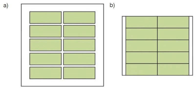
Fig. 3. Overview of (a) a milled panel with fixing pads and (b) a scored panel
If the edges must be chamfered, it is best to lay out the PCBs in the panel to have the edges located outwards and available for skipping. Chamfered edges inside the panel will most likely require cost-inflating processing by Z-routing with a tapered mill.
The minimum hole diameters specified in the designs is another PCB price defining actor. For example, TS PCB is a manufacturer who applies a standard finished hole diameter of 0.4 mm. This means that smaller diameter values will increase the PCB price inversely to the minimum hole diameter. Hence it is recommended to apply 0.4 mm or larger holes to keep a low price.
Adding other operations to the design, e.g. carbon prints / peelable masks or plugged vias will also affect the PCB pricing. It is indeed difficult to imagine a design being delivered without the solder masks replaced, but via plugging can be replaced with much cheaper solder mask casting, if the via holes are small enough (0.2 mm max.). This via finish will reliably protect their voids, unlike in open vias. If, however, via plugging is necessary, the price can be reduced by doing without flat via surfaces; although visually better for the PCB, smooth surfaces also complicate the plugging process.
The soldering resist colour matters too
The PCB pricing may even be affected (to a small extent) by the solder mask/resist colour. The standard green solder masks, also known as photomasks, is deposited with the curtain coating process on an automated line which guarantees uniform thickness of the layer. The mask is developed in a photochemical process, which assures precise alignment with the mosaics. Many PCB manufacturers, including TS PCB, offer a wide range of solder resist colours. The colours other than green are applied in a hand silkscreen process, which is more time-consuming and may result in slight offsets of the masks relative to the copper mosaic. The standard green solder masks help providing low price products.
Summary
The paper discusses the most price-relevant processing parameters of printed circuit boards. Each parameter is presented with cost-effective alternatives. Price optimisation can certainly be facilitated by requesting PCB quotations. The PCB manufacturer will specify what design processing parameters are predominant in the PCB price and advise what modifications can reduce the PCB price.
31.08.2017
Frank-apollopcb
Dear Dariusz Zaleski, Thanks fo ryour detailed sharing of most significant PCB parameters that condition the prices,I read through your article,I think this factors you talking mostly focus on base material paremeters and design step,and I agree with you about them,how about after designed PCBs,also I think many factors can reduce the cost when you process them.I think the PCB making solution and area also greatly reduce the PCB price. I summarize from the actually process from APOLLOPCB. 1,ONE STOP PROCESS MACHINE,in the early twentieth century, many PCB industry professionals to realize that if there is a machine capable of disposable produced circuit boards, without the need for complicated processes and process waiting time, please note that the process of making the board is not less, the only one good chance in the set procedures, the circuit board from the initial raw material to the finished pcbs are produced in only one machine,without traditional workers,greatly short the waiting time bettwen each process.Thus reduce the labor cost and time. 2,PANELIZATION WITH DIFFERENT DESIGN,Traditional crafts, one design PCB needs one set-up, two sets of film, a process mold, a test mold,those are all necessary even you only produce 1 pcs of PCB.The cost is extremly high comparing with updated process way.PANELIZATION WITH DIFFERENT DESIGN.some time we can panelize 20 different designs in one panel,sahring one set-up,2 film,process mold and test mold.The limite of panelization with different design is those 20 different design need same technical parameters.So one company only can do this based on they have thousand of customers that may need same technical parameters of PCBs. Frank wang Engineer services in APOLLOPCB www.apollopcb.com