Printed circuits. Typical errors in production documentation. Part 2
25.11.2015

The first part of the article (see "Elektronik" issue 3/15) is dedicated to the characteristics of good production documentation and the popular file formats used in the PCB industry. Typical errors of project/design documentation were also discussed as exhibited on mosaic, resists and text layers. Defects of mechanical treatment documentation were also characterised in detail.
This part presents the typical construction abnormalities in automated assembly PCB panels, their negative effects, and guidelines for the design of panels that prevent problems in the manufacture and assembly of packs. The end of this article presents the typical omissions found in the specifications of design processing parameters and build-ups of multilayer circuits.
Construction of circuit boards
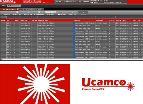
Image 1. Example of a scored board with two circuits.
The majority of printed circuit boards (PCBs), especially in moderate and large production series, is located on board panels to handle the processing on the automatic assembly lines. The panels are either designed by customers or by the PCB manufacturers to customer's specifications. If a customer needs a PCB panelized but does not provide any specifications, the panel is composed by the manufacturer according to the design processing parameters and in-house experience.
Unfortunately, not all custom panels are composed properly, and the typical errors may result in, among others, warping of the laminate or breakage (depanelization) already at the manufacturing stage. Moreover, an erroneous design may also result in other problems during component assembly, soldering, or depanelization of the assembled packs.
A properly designed panel features the maximum attainable rigidity which assures it will retain integrity during manufacturing machining and counters excessive bending of the laminate under the weight of components during assembly and soldering. Maximally easy machining of panels is also desired.
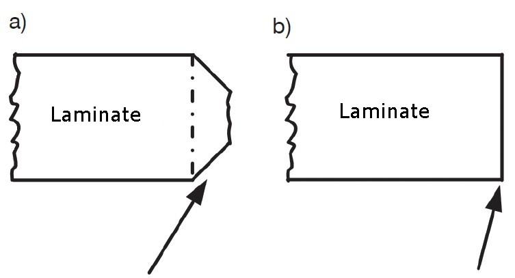
Fig. 1. Comparison of edges in (a) scored and (b) milled PCBs.
The simplest panel type that meets these criteria feature circuits that are scored only (see Image 1). Scored panels feature high rigidity, especially with thick laminates (1 mm and higher), and are intended for circuits with rectangular forms made on laminates at least 0.5 mm thick, where the mosaics do not directly touch the outline but are offset by 0.1 to 0.5 mm, depending on the actual laminate thickness. The drawback of those panels is that the dimensional tolerance is poor when compared with milled panels, since it results from the precision of scoring and the circuit edges are not perfectly square (see Fig. 1).
If a scored panel will feature different PCBs, their location layout must be carefully thought out. Fig. 2a shows an incorrect construction of the discussed panel type. The scoring of smaller circuits will damage the surfaces of larger circuits, since skipping requires a certain run out length before the scoring saw stops and rises. This example design can be corrected by simply separate the circuit lines with a 10 mm high laminate strip to protect the lower circuit line from notching when the top line will be scored (see Fig. 2b).
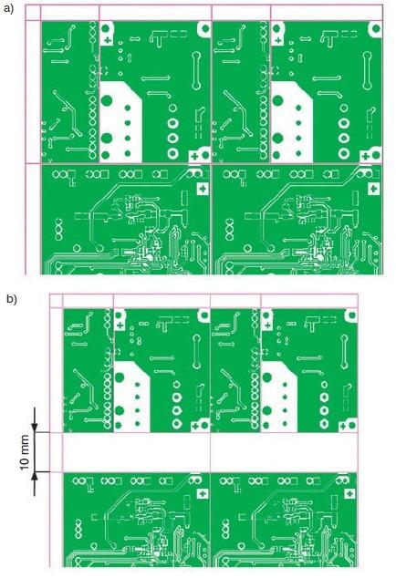
Fig. 2. Piece of (a) an incorrect and (b) properly arranged scored panels with many boards.
The panels for laminates that are less than 0.8 mm and/or feature irregular outline forms shall be designed for milling with fixing tabs (see Image 2). Milled panels are also used when circuit dimensions and tolerances are critical. To assure high rigidity and easy depanelizing of assembled packs, the circuits are held within the panel by fixing tabs which are drilled (perforated) on the circuit edge end. Image 3 shows an example of a fixing tab.
The number of fixing tabs determines the overall panel rigidity. The recommended maximum spacing of fixing tabs is 5 cm along the circumference outline for the typical 1.55 mm thick laminates. The fixing tab spacing must be reduced for thinner laminates, while a spacing of 6 or 7 cm is allowed for thicker laminates. When laying out the fixed tabs, remember that they cannot be located along the plated circuit edges and must follow other restrictions imposed by downstream assembly operations.
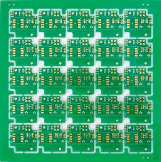
Image 2. Overview of a milled panel example.
The more limited dimension a panel has, the stiffer it is. The size must be reduced accordingly to the reduction of laminate thickness. The panel size must not be less than the size of a single circuit. On the other hand, the maximum permissible panel size is limited by the working area of the automated assembly line, the panel construction rigidity and the working field of the formats applied by the PCB manufacturer in question. It is a good practice to construct panel in sizes approximate to the A4 paper size or lower.
Panels are usually given margins, which are additional laminate strips located along the long panel edges, or frames around the panel outer edges. These extra components have several uses: (i) increase the panel rigidity, (ii) serve as work areas of the assembly line handling feeders, and (iii) carry the fiducial markers for the automatic assemblers. It is important to locate the fiducials in places that will protect them from damage during panel machining.
Sometimes mixed processing panels are designed with the straight runs of circuit edges made by scoring and irregular runs made by milling. In this case do not compose scored circuits that have cuts within the outline, since it will be impossible to precisely manufacture the circuit. This effect is shown in Fig. 3a; the pointers show the locations that will have milling residues. An exception to this rule are circuits with symmetric cuts on opposite sides that can be laid with the edges butted for scoring (see Fig. 3b) while retaining a high accuracy of milling.
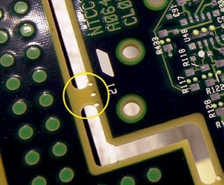
Image 3. Example of a single-perforated fixing tab (in the yellow oval).
The panel construction must also include the components the pieces of extend outside of the post-assembly circuit area. These designs should have additional clearances provided between the adjacent lines and columns of the panel circuits. Butting a scored panel in this case will prevent assembly of the areas obscured by the components already installed on adjacent circuits.
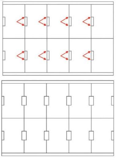
Fig. 3. (a) Incorrect and (b) correct composition of boards with cuts in a scored panel.
Sometimes the one-off PCBs must be manufactured on a panel if the single piece is extremely small (i.e. less than 30 mm in size). Machining one-off circuits so small is challenging or outright impossible. In this case the panel is constructed by the PCB manufacturer and consulted with the customer.
Processing specification errors
As already said in the first part of this article, the production documentation should cover a single processing specification (i.e. the processing sheet) the records of which can be construed in an explicit manner. The typical flaws of specification are errors in the provisions for the required layer thickness of copper and the laminate, and the build-up descriptions of multilayer PCBs. The design technology can also be explained in insufficient detail.
Thickness of copper layers
The thickness of copper layers specified in processing sheets is understood by PCB manufacturers (and TS PCB too) as the target (finished) values, unless the customer specifies that the parameter applies to the base copper, which is the copper foil thickness of the raw laminate. The finished thickness of copper layers is the ultimate mosaic thickness of the finished PCBs, and in plated PCBs (i.e. double-sided and multilayer PCBs), it is the total of the laminate base copper thickness and the galvanic Cu thickness (which ranges from 25 to 30 µm). This means that double-sided PCBs with the standard 35 µm thick finish copper are manufactured from 18 µm thick base copper laminates, and the finished copper thickness of 18 µm cannot be obtained.
In single-sided PCBs and multilayer PCB cores the standard laminate has the Cu foil with 35 µm base copper; this value is the finished value too, because the laminates are not plated. It is then possible to have single-sided PCBs with 18 µm finish copper thickness, since they can be manufactured from the base laminate for double-sided PCBs.
It is best to use the target (finished) copper thickness value in the processing sheet. Sometimes customers use the base copper thickness values by mistake, believing that it is also the target copper value. This error can be sometimes detected by the PCB manufacturers; however, in majority of those cases the PCBs are manufactured at higher thickness that departs from the customer needs. This inflates the PCB costs and may affect the performance of the electronic circuits with the transmission lines at the designed impedance values.
Laminate thickness
Not unlike in the mosaics, the laminates also have base thickness and finished thickness. Base thickness is the original thickness of the laminate input to production and includes the Cu foil thickness if single and double-sided PCBs are manufactured; note that this does not apply to multilayer PCB cores. The finished laminate thickness is then increased by the coats deposited during the manufacturing process: galvanic copper, plating (tin or gold) and resists.
If the finished laminate thickness is not critical, it is best to use the base laminate thickness and tolerance value in the processing sheets. Whereas if the PCB thickness is critical in a design, the customer concerned should consult the thickness of deposited coats and specify the expected finished laminate thickness with tolerance in the processing sheet. The average coat thickness depend on the design technology and available in the technology specification of PCB manufacturers. Sometimes PCB manufacturers clarify the designs, since an increase of laminate thickness by deposition of successive layers may prevent reaching the customer's specified finished thickness.
Build-ups of multilayer PCBs
The build-up parameters of multilayer PCBs, i.e. the cross-section which shows the arrangement and types of individual layers should consider at the design stage the processing capacity and material range at the disposal of the concerned PCB manufacturer. Highly non-standard or highly sophisticated cores and prepregs (pre-impregnated materials made of mixtures of resin and glass fibres) and/or their arrangement may, in extreme cases, render production of the designed PCB infeasible. In this case PCB manufacturers usually propose alternative build-ups the parameters of which are as approximate to the original one as possible and based on materials in stock. If a customer rejects the alternative(s), the project lead time and labour consumption will grow, because non-standard materials must be ordered, unless other processing requirements completely preclude the manufacturability of PCBs.
It is well worth it to design build-ups that are symmetrical to the cross-section centre, since the surface stresses will be approximate on both sides of the laminate. Symmetrical build-ups are sometimes impossible. For example, this can be caused by very specific mosaic impedance values, resulting in warping of finished PCBs during soldering on the assembly line. This effect is caused varying surface stresses in the laminate that result from the asymmetrical structure.
Another problem in the build-up design is the number and types of prepregs. The majority of PCB manufacturers, including TS PCB, recommends at least two isolating prepregs between adjacent conductor layers; a single prepreg greatly increases the risk of delamination. On the other hand, the maximum prepreg count is limited by the laminate thickness after pressing. Note that the thicker the copper layers are, the more prepregs must be used to assure an optimum resin fill level in copper-free areas, and to minimise the risk of delamination. Hence it is impossible to produce multilayer PCBs 0.8 mm thick or less with 105 µm copper layers. In order to avoid excessive thickness increase at the same time, the recommended prepreg should be the thinnest possible, i.e. type 1080 (3.04 mils), which also exhibits a high resin saturation level. It is also a good practice to have the highest possible copper fill levels within the inner layers. This favours successful laminate pressing.
PCBs with blind vias exhibit a dependence of the blind via diameter on the permissible drilling depth, which results with the possible number of layers to be connected. Blind vias can be reduced in size with the minimum spacing of joined layers. It is recommended to use blind vias in thin laminates (less than 1 mm thick), unless there are other contraindications. If a higher thickness is desired, it is better to design the PCB with the blind rivets joining only the outer layers with their nearest inner layers, separate the layers with two 1080 prepregs, and produce the designed finished thickness of the laminate by applying thicker cores.
Missing sequences of inner layers is yet another error found in multilayer PCB documentation. This data can be provided with suitable nomenclature of the mosaic files, by numbering the layers of the mosaics, or in a text description appended to the specifications. The layer arrangement may be critical, especially in fast high-frequency digital circuits which feature transmission lines with matched impedance values. A design devoid of such information will certainly be reported by the PCB manufacturer for clarification.
Summary
The article discusses typical errors in electronic production documents that affect its quality, a basic condition of project lead times and costs. Providing PCB manufacturers with too many specification files, using wrong file formats, or vague (or even contradictory) information about the manufacturing technology greatly obstruct design production preparation, create great problems with interpretation of actual customer requirements and extend the design production lead times due to the necessary clarification and supplementation of data.