Construction of multi-layer PCB's

Core, prepreg & copper foil.
Multi-layer printed circuits, when compared to single or double-layer circuits, exhibit a more complex layer structure.
An example stackup is shown in Fig. 1 which presents the layer stack of a typical 4-layer circuit. It is made up of three basic elements: core (1), prepregs (2) and copper foils (3).
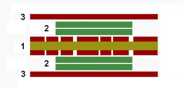
Fig. 1. Typical structure of a 4-layer circuit.
Definitions of specific elements are presented below:
Core– double-sided laminate on whose copper layers internal layers of multi-layer circuits are represented. Thickness of the copper foil is mostly the target thickness as it usually does not go through the copper-plating process to the exception of circuits with vias. A typical 4-layer circuit is based on a single core, a 6-layer circuit on two core and 8-layer circuit on three cores.
Prepreg - is a laminate semi-finished product consisting of composite fibres soaked in resin. Its major task is to guarantee the durable gluing of specific layers of a multi-layer circuit in the ironing process. The most popular prepregs include: 1080, 2125 (now withdrawn), 2116, 7628 characterised by varying thickness, degree of filling with resin and warp density. The prepregs mentioned above are also available in HR (high resin) versions. In order to guarantee correct connection between all the layers and thus high quality of circuits (without delamination) at least two prepregs need to be used between specific layers of copper (among others things, guaranteeing a sufficient amount of resin).
Copper foil – a sheet of copper foil prepared for the ironing process. On one side the sheet is rough (it has a complex structure) to guarantee good grip to the prepreg. Its thickness is always smaller than the required target thickness because an additional layer of copper is still applied in the metal-plating process (copper-plated). Usually, the added copper layer is 20 to 25 um thick.
02.05.2018
[TS PCB] Katarzyna Lenczewska
Hello Henderb! Thank you for letting us know. Picture is already fixed.
01.05.2018
Henderb
Hi, great article.
However the Fig. 1 is no shown. I tried with Firefox and Chrome browsers. Please fix it.
Thanks in advance,
Henderb


 comments (2)
